SNVS424D January   2006  – December 2014 LM5106

PRODUCTION DATA.  

  1. Features
  2. Applications
  3. Description
  4. Revision History
  5. Pin Configuration and Functions
  6. Specifications
    1. 6.1 Absolute Maximum Ratings
    2. 6.2 ESD Ratings
    3. 6.3 Recommended Operating Conditions
    4. 6.4 Thermal Information
    5. 6.5 Electrical Characteristics
    6. 6.6 Switching Characteristics
    7. 6.7 Typical Characteristics
  7. Detailed Description
    1. 7.1 Overview
    2. 7.2 Functional Block Diagram
    3. 7.3 Feature Description
      1. 7.3.1 Start-up and UVLO
    4. 7.4 Device Functional Modes
  8. Application and Implementation
    1. 8.1 Application Information
    2. 8.2 Typical Application
      1. 8.2.1 Design Requirements
      2. 8.2.2 Detailed Design Procedure
        1. 8.2.2.1 Detailed Design Procedure
      3. 8.2.3 Application Curves
  9. Power Supply Recommendations
    1. 9.1 Power Dissipation Considerations
  10. 10Layout
    1. 10.1 Layout Guidelines
      1. 10.1.1 HS Transient Voltages Below Ground
    2. 10.2 Layout Example
  11. 11Device and Documentation Support
    1. 11.1 Trademarks
    2. 11.2 Electrostatic Discharge Caution
    3. 11.3 Glossary
  12. 12Mechanical, Packaging, and Orderable Information

封装选项

机械数据 (封装 | 引脚)
散热焊盘机械数据 (封装 | 引脚)
订购信息

9 Power Supply Recommendations

9.1 Power Dissipation Considerations

The total IC power dissipation is the sum of the gate driver losses and the bootstrap diode losses. The gate driver losses are related to the switching frequency (f), output load capacitance on LO and HO (CL), and supply voltage (VDD) and can be roughly calculated as:

Equation 12. PDGATES = 2 • f • CL • VDD2

There are some additional losses in the gate drivers due to the internal CMOS stages used to buffer the LO and HO outputs. Figure 20 shows the measured gate driver power dissipation versus frequency and load capacitance. At higher frequencies and load capacitance values, the power dissipation is dominated by the power losses driving the output loads and agrees well with the Equation 12. This plot can be used to approximate the power losses due to the gate drivers.

20175905.gif
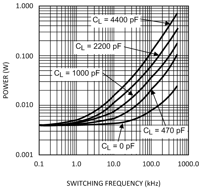
Figure 20. Gate Driver Power Dissipation (LO + HO)
VCC = 12 V