SNVS424D January 2006 – December 2014 LM5106
PRODUCTION DATA.
7 Detailed Description
7.1 Overview
The LM5106 is a single PWM input gate driver with Enable that offers a programmable dead-time. The dead-time is set with a resistor at the RDT pin and can be adjusted from 100 ns to 600 ns. The wide dead-time programming range provides the flexibility to optimize drive signal timing for a wide range of MOSFETs and applications.
The RDT pin is biased at 3 V and current limited to 1 mA maximum programming current. The time delay generator will accommodate resistor values from 5k to 100k with a dead-time time that is proportional to the RDT resistance. Grounding the RDT pin programs the LM5106 to drive both outputs with minimum dead-time.
7.2 Functional Block Diagram
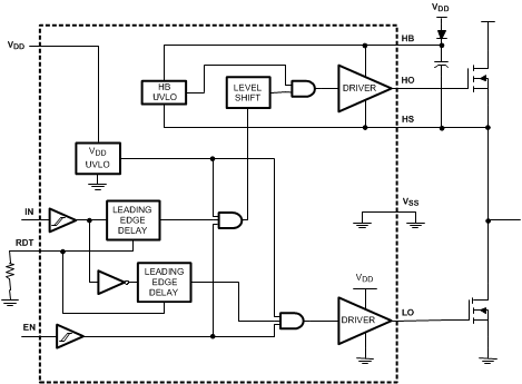
7.3 Feature Description
7.3.1 Start-up and UVLO
Both top and bottom drivers include undervoltage lockout (UVLO) protection circuitry which monitors the supply voltage (VDD) and bootstrap capacitor voltage (HB – HS) independently. The UVLO circuit inhibits each driver until sufficient supply voltage is available to turn on the external MOSFETs, and the UVLO hysteresis prevents chattering during supply voltage transitions. When the supply voltage is applied to the VDD pin of the LM5106, the top and bottom gates are held low until VDD exceeds the UVLO threshold, typically about 6.9 V. Any UVLO condition on the bootstrap capacitor will disable only the high-side output (HO).
7.4 Device Functional Modes
| EN | IN Pin | LO Pin | HO Pin |
|---|---|---|---|
| L | Any | L | L |
| H | H | L | H |
| H | L | H | L |