ZHCSM35F January 2007 – May 2021 LM5002
PRODUCTION DATA
- 1 特性
- 2 应用
- 3 说明
- 4 Revision History
- 5 Pin Configuration and Functions
- 6 Specifications
- 7 Detailed Description
- 8 Application and Implementation
- 9 Power Supply Recommendations
- 10Layout
- 11Device and Documentation Support
- 12Mechanical, Packaging, and Orderable Information
8.2.1.2.5 Output Diode Rating
The average diode current equals the output current under normal circumstances, but the diode must be designed to handle a continuous current limit condition for the worst case:
Equation 12. 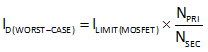
where:
- ILIMIT(MOSFET) is the peak current limit of the interal MOSFET of the LM5002
The maximum reverse voltage applied to the diode occurs during the MOSFET on time in Equation 13.
Equation 13. 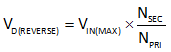
The diode's reverse capacitance resonates with the transformer inductance (and other parasitic elements) to some degree and causing ringing that may affect conducted and ratiated emissions compliance. Usually an RC snubber network across the diode anode and cathode cam eliminate the ringing.