ZHCSHN2B February   2010  – February 2018 LM48580

PRODUCTION DATA.  

  1. 特性
  2. 应用
  3. 说明
    1.     Device Images
      1.      典型应用
  4. 修订历史记录
  5. Pin Configuration and Functions
    1.     Pin Functions
  6. Specifications
    1. 6.1 Absolute Maximum Ratings
    2. 6.2 ESD Ratings
    3. 6.3 Recommended Operating Conditions
    4. 6.4 Thermal Information
    5. 6.5 Electrical Characteristics: VDD = 3.6 V
    6. 6.6 Typical Performance Characteristics
  7. Parameter Measurement Information
  8. Detailed Description
    1. 8.1 Overview
    2. 8.2 Functional Block Diagram
    3. 8.3 Feature Description
      1. 8.3.1 Class H Operation
      2. 8.3.2 Properties of Piezoelectric Elements
      3. 8.3.3 Differential Amplifier Explanation
      4. 8.3.4 Thermal Shutdown
      5. 8.3.5 Gain Setting
    4. 8.4 Device Functional Modes
      1. 8.4.1 Shutdown Function
  9. Application and Implementation
    1. 9.1 Application Information
    2. 9.2 Typical Application
      1. 9.2.1 Design Requirements
        1. 9.2.1.1 Proper Selection of External Components
          1. 9.2.1.1.1 Boost Converter Capacitor Selection
      2. 9.2.2 Detailed Design Procedure
        1. 9.2.2.1 Boost Converter Output Capacitor Selection
          1. 9.2.2.1.1 Inductor Selection
          2. 9.2.2.1.2 Diode Selection
        2. 9.2.2.2 Application Curves
  10. 10Power Supply Recommendations
  11. 11Layout
    1. 11.1 Layout Guidelines
    2. 11.2 Layout Example
  12. 12器件和文档支持
    1. 12.1 器件支持
      1. 12.1.1 开发支持
        1. 12.1.1.1 第三方产品免责声明
    2. 12.2 接收文档更新通知
    3. 12.3 社区资源
    4. 12.4 商标
    5. 12.5 静电放电警告
    6. 12.6 Glossary
  13. 13机械、封装和可订购信息

封装选项

机械数据 (封装 | 引脚)
散热焊盘机械数据 (封装 | 引脚)
订购信息

Typical Performance Characteristics

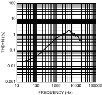
LM48580 30108011.gif
VDD = 3.6 V VOUT = 9 VP-P RL = 6 μF + 10 Ω
Figure 1. THD+N vs Frequency
LM48580 30108013.gif
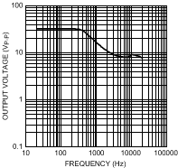
VDD = 3.6 V THD+N = 5% RL = 6 μF + 10 Ω
Figure 3. Output Voltage vs Frequency
LM48580 30108009.gif
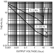
VDD = 3.6 V RL = 6 μF + 10 Ω
Figure 5. THD+N vs Output Voltage
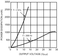
LM48580 30108015.gif
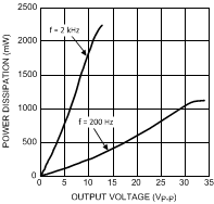
VDD = 3.6 V RL = 6 μF + 10 Ω
Figure 7. Power Consumption vs Output Voltage
LM48580 30108017.gif
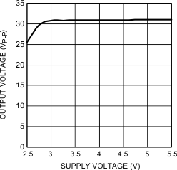
RL = 6 μF + 10 Ω, f = 200 Hz
Figure 9. Output Voltage vs Supply Voltage
LM48580 30108019.gif
VDD = 3.6 V VCM = 1 VP-P RL = 6 μF + 10 Ω
Figure 11. CMRR vs Frequency
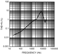
LM48580 30108012.gif
VDD = 4.2 V VOUT = 10 VP-P RL = 6 μF + 10 Ω
Figure 2. THD+N vs Frequency
LM48580 30108014.gif
VDD = 4.2 V THD+N = 5% RL = 6 μF + 10 Ω
Figure 4. Output Voltage vs Frequency
LM48580 30108010.gif
VDD = 4.2 V RL = 6 μF + 10 Ω
Figure 6. THD+N vs Output Voltage
LM48580 30108016.gif
VDD = 4.2 V RL = 6 μF + 10 Ω
Figure 8. Power Consumption vs Output Voltage
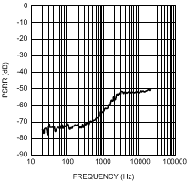
LM48580 30108019.gif
VDD = 3.6 V f = 200 Hz RL = 6 μF + 10 Ω,
VRIPPLE = 200 mVP-P
Figure 10. PSRR vs Frequency