ZHCSF89B June 2011 – June 2016 LM3559
PRODUCTION DATA.
- 1 特性
- 2 应用
- 3 说明
- 4 修订历史记录
- 5 Pin Configuration and Functions
- 6 Specifications
-
7 Detailed Description
- 7.1 Overview
- 7.2 Functional Block Diagram
- 7.3
Feature Description
- 7.3.1 Power Amplifier Synchronization (TX1)
- 7.3.2 Input Voltage Flash Monitor Fault
- 7.3.3 Independent LED Control
- 7.3.4 Hardware Torch
- 7.3.5 Fault Protections
- 7.3.6 Input Voltage (VIN ) Monitor
- 7.3.7 VIN Flash Monitor (Flash Current Rising)
- 7.3.8 Last Flash Register
- 7.3.9 LED Voltage Monitor
- 7.3.10 ADC Delay
- 7.3.11 Flags Register and Fault Indicators
- 7.4
Device Functional Modes
- 7.4.1 Start-Up (Enabling the Device)
- 7.4.2 Pass Mode
- 7.4.3 Flash Mode
- 7.4.4 Torch Mode
- 7.4.5 Privacy-Indicate Mode
- 7.4.6 GPIO1 Mode
- 7.4.7 TX2/INT/GPIO2
- 7.4.8 TX2 Mode
- 7.4.9 GPIO2 Mode
- 7.4.10 Interrupt Output (INT Mode)
- 7.4.11 NTC Mode
- 7.4.12 Alternate External Torch (AET Mode)
- 7.4.13 Automatic Conversion Mode
- 7.4.14 Manual Conversion Mode
- 7.5 Programming
- 7.6
Register Maps
- 7.6.1 Enable Register
- 7.6.2 Torch Brightness Register
- 7.6.3 Flash Brightness Register
- 7.6.4 Flash Duration Register
- 7.6.5 Flags Register
- 7.6.6 Configuration Register 1
- 7.6.7 Configuration Register 2
- 7.6.8 GPIO Register
- 7.6.9 Last Flash Register
- 7.6.10 VLED Monitor Register
- 7.6.11 ADC Delay Register
- 7.6.12 Input Voltage Monitor Register
- 7.6.13 Privacy Register
- 7.6.14 Privacy PWM Period Register
- 7.6.15 Indicator Register
- 7.6.16 Indicator Blinking Register
- 8 Application and Implementation
- 9 Power Supply Recommendations
- 10Layout
- 11器件和文档支持
- 12机械、封装和可订购信息
10 Layout
10.1 Layout Guidelines
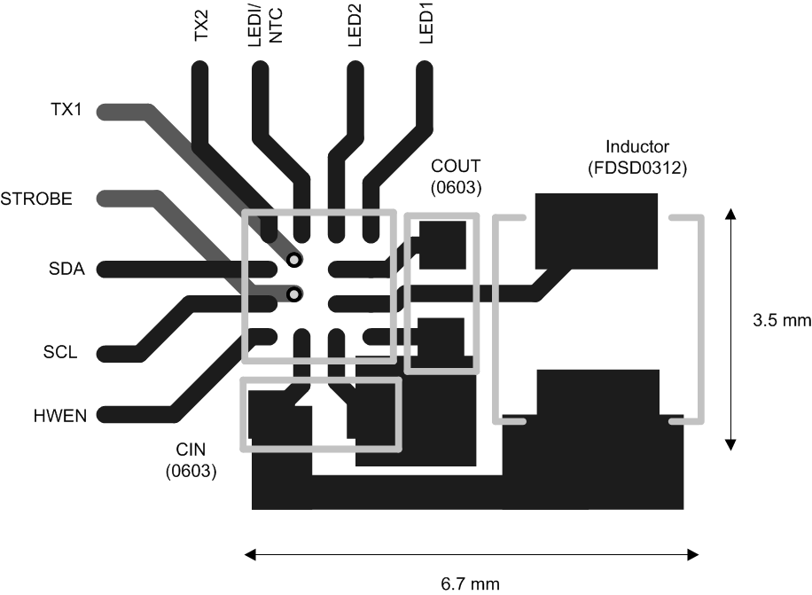
The high switching frequency and large switching currents of the LM3559 make the choice of layout important. The following steps should be used as a reference to ensure the device is stable and maintains proper LED current regulation across its intended operating voltage and current range.
- Place CIN on the top layer (same layer as the LM3559) and as close as possible to the device. The input capacitor conducts the driver currents during the low side MOSFET turnon and turnoff and can detect current spikes over 1 A in amplitude. Connecting the input capacitor through short wide traces to both the IN and GND terminals reduces the inductive voltage spikes that occur during switching and which can corrupt the VIN line.
- Place COUT on the top layer (same layer as the LM3559) and as close as possible to the OUT and GND pins. The returns for both CIN and COUT must come together at one point, and as close as possible to the GND pin. Connecting COUT through short wide traces will reduce the series inductance on the OUT and GND pins that can corrupt the VOUT and GND line and cause excessive noise in the device and surrounding circuitry.
- Connect the inductor on the top layer close to the SW pin. There must be a low-impedance connection from the inductor to SW due to the large DC inductor current and, at the same time, the area occupied by the SW node must be small to reduce the capacitive coupling of the high dV/dt present at SW that can couple into nearby traces.
- Avoid routing logic traces near the SW node to avoid any capacitively coupled voltages from SW onto any high impedance logic lines such as TX1/TORCH/GPIO1, TX2/INT/GPIO2, HWEN, LEDI/NTC (NTC mode), SDA, and SCL. A good approach is to insert an inner layer GND plane underneath the SW node and between any nearby routed traces. This creates a shield from the electric field generated at SW.
- Terminate the flash LED cathodes directly to the GND pin of the LM3559. If possible, route the LED returns with a dedicated path to keep the high amplitude LED currents out of the GND plane. For flash LEDs that are routed relatively far away from the LM3559, a good approach is to sandwich the forward and return current paths over the top of each other on two layers. This helps to reduce the inductance of the LED current paths.
- The NTC thermistor is intended to have its return path connected to the LEDs cathode. This allows the thermistor resistive divider voltage (VNTC) to trip the comparators threshold as VNTC is falling. Additionally, the thermistor-to-LED cathode junction must be connected as closely as possible in order to reduce the thermal impedance between the LED and the thermistor. The drawback is that the return of the thermistor may detect the switching currents from the device boost converter. Because of this, it is necessary to have a filter capacitor at the NTC pin which terminates close to the GND of the LM3559 (see CBYP in Figure 48).
10.2 Layout Example
 Figure 50. LM3559 Layout Example