ZHCSBI0C March 2013 – October 2014 LM3279
PRODUCTION DATA.
- 1 特性
- 2 应用
- 3 说明
- 4 修订历史记录
- 5 Pin Configuration and Functions
- 6 Specifications
- 7 Detailed Description
- 8 Application and Implementation
- 9 Power Supply Recommendations
- 10Layout
- 11器件和文档支持
- 12机械、封装和可订购信息
7 Detailed Description
7.1 Overview
The LM3279 buck-boost converter provides high-efficiency, low-noise power for RF power amplifiers (PAs) in mobile phones, portable communicators and similar battery powered RF devices. It is designed to allow the RF PA to operate at maximum efficiency for a wide range of power levels from a single Li-Ion battery cell. The capability of LM3279 to provide an output voltage lower than as well as higher than the input battery voltage enables the PA to operate with high linearity for a wide range of battery voltages, thereby extending the usable voltage range of the battery. The converter feedback loop is internally compensated for both buck and boost operation, and the architecture is such that it provides seamless transition between buck and boost mode of operation. The LM3279 operates in energy-saving Pulse Frequency Modulation (PFM) mode for increased efficiencies and current savings during low-power RF transmission modes. The output voltage is dynamically programmable from 0.4 V to 4.2 V by either programming the VSET value in register 00h, or adjusting the voltage on the control pin VCON. The fast output voltage transient response of LM3279 makes it suitable for adaptively adjusting the PA supply voltage depending on its transmitting power which improves systems efficiency and prolongs battery life
Additional features include current-overload protection, output overvoltage clamp, and thermal-overload shutdown.
The LM3279 is constructed using a chip-scale 16-bump DSBGA package that offers the smallest possible size for space-critical applications such as cell phones where board area is an important design consideration. Use of a high switching frequency (2.4 MHz, typ.) reduces the size of external components. As shown in Figure 24 and Figure 27, only three external power components are required for circuit operation. Use of a DSBGA package requires special design considerations for implementation. (See DSBGA Package Assembly And Use in the Layout section.) Its fine bump-pitch requires careful board design and precision assembly equipment. Use of this package is best suited for opaque-case applications where its edges are not subjected to high-intensity ambient red or infrared light. In addition, the system controller should set VIO = LOW (or EN if system implementation with analog VCON) during power-up and other low supply-voltage conditions.
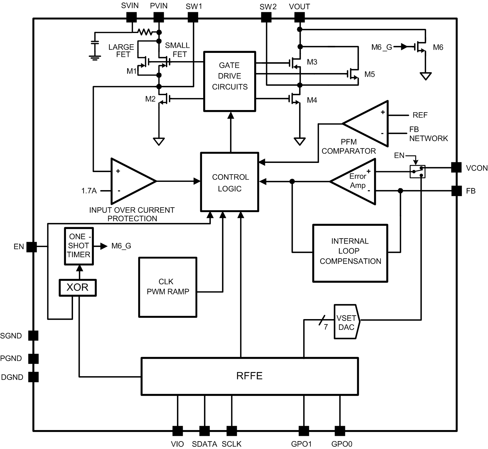
7.2 Functional Block Diagram

7.3 Feature Description
7.3.1 Dynamically Adjustable Output Voltage
The LM3279 features a dynamically adjustable output voltage to eliminate the need for external feedback resistors. The output can be set from 0.4 V to 4.2 V by either programming the VSET value in register 00h, or by changing the voltage on the analog VCON pin when implementing analog control. This feature is useful in cell-phone RF PA applications where peak power is needed only when the handset is far away from the base station or when data is being transmitted. In other instances, the transmitting power can be reduced. Hence, the supply voltage to the PA can be reduced, promoting longer battery life. In order to adaptively adjust the supply voltage to the PA in real time in a cell-phone application, the output-voltage transition should be fast enough in order to meet the RF transmit signal specifications. The LM3279 offers ultra-fast output-voltage transition without drawing very large currents from the battery supply. For a current limit of 1700 mA (typ.), the output voltage can transition from 0.6 V to 3.4 V in less than 20 µs with a load resistance of 5 Ω at VBATT = 3.8 V.
7.3.2 Seamless Mode Transition
In a typical non-inverting buck-boost converter, all four power switches M1 through M4 are switched every cycle. This operation increases MOSFET drive losses and lowers the converter efficiency. The LM3279 switches only two power switches every cycle to improve converter efficiency. Hence, it operates either as buck converter or a boost converter depending upon the input and output voltage conditions. This creates a boundary between the buck and boost mode of operation. When the input battery voltage is close to the set output voltage, the converter automatically switches to a four-switch operation seamlessly such that the output voltage does not see any perturbations at the mode boundary. The excellent mode-transition capability of the LM3279 enables low-noise output with highest efficiency. Internal feedback loop compensation ensures stable operation in buck, boost, and buck-boost modes, as well as during mode transitions.
7.3.3 Setting The Output Voltage
The output voltage can be set by two methods: via Analog Control or Digital Control.
In the Analog Control method, the VCON pin is an external analog control input pin. It can be enabled (EN = HIGH) or disabled (EN = LOW). An analog voltage is provided by an external MCU (either a D/A or averaged PWM output) to the VCON pin. The range of this signal is 0.167V (min.) to 1.4V (max. typ.) to provide the full range of the possible output voltage. This signal is internally amplified by a gain of 3 to go from 0.5V to 4.2V output.
For the Digital Control method, the output voltage is set by writing a 7-bit value to reg 00h, bits 0 through 6. Programming a value 00h will force the LM3279 into low-power mode where the entire device except the RFFE interface is turned off. Programming register 00h with the value 02h will place the LM3279 into Standby mode where the SW pin is tri-stated. Values programmed above 0Bh will determine the output voltage from 0.4 V to 4.212 V in 36 mV (typ.) increments.
The output voltage quickly adjusts to the new output voltage value within 20 microseconds both in the positive and negative directions. To accomplish this, the LM3279 buck-boost output can both source and sink current. In the positive direction the buck may assume a 100-percent duty cycle or enter boost mode at up to 50% duty cycle to provide the required current. In the negative direction, the synchronous rectifier (NFET) will remain on to sink current from the output capacitor.
7.3.4 General Purpose Outputs
The LM3279 provides two general-purpose outputs to control the RF front-end circuitry. These outputs have a maximum output voltage of 1.8 V. These bits are set by writing to register 02h bits 6 (GPO1) and bit 7 (GPO0).
7.3.5 VCONON
When EN = HIGH, the output is disabled when VCON is below 125 mV (typ.). It is enabled when VCON is above 150 mV (typ.). The threshold has 25 mV (typ.) of hysteresis.
7.3.6 RDSON Management
The LM3279 has a unique RDSON-management function to improve efficiency in both the low-output voltage and high-output voltage conditions. For VSET < 2.1 V (typ.) or VCON < 0.7 V (typ.), the device uses only a small part of the PMOSFET M1 to minimize drive loss of the PMOSFET. When VSET > 2.175 V or VCON > 0.725 V, a large PMOSFET is also used along with the small PMOSFET. The threshold has a 25 mV of hysteresis. For RF PAs, the current consumption typically increases with its supply voltage; thus, higher supply voltage for a PA also means higher power delivered to it. Hence, adding a large PMOSFET for VSET > 2.175 V or VCON > 0.725 V reduces the conduction losses, thereby achieving high efficiency. The LM3279 can also provide output voltages higher than the battery voltage. This boost mode of operation is typically used when the battery voltage has discharged to a low voltage that is not sufficient to provide the required linearity in the PA. A special RDSON-management scheme is designed for operation well into boost mode so that an auxiliary PMOSFET switch is also turned on along with Large and Small PMOSFET switches, effectively reducing the RDSON of M1 to a very low value in order to keep the efficiency maximum. Since M1 conducts all the time in boost mode, reducing the RDSON of M1 achieves significant improvement in efficiency.
7.3.7 Supply Current Limit
A current limit feature allows the LM3279 to protect itself and external components during overload conditions. In Pulse Width Modulation (PWM) mode, a 1700 mA (typ.) cycle-by-cycle current limit is normally used when VOUT is above 2.1 V (typ.) and an 850 mA (typ.) limit is used when VOUT is below 2.1 V (typ.). If an excessive load pulls the output voltage down to approximately 0.30 V, the device switches to a timed current-limit mode, and the current limit in this mode is 850 mA (typ.), independent of the set VOUT voltage. In timed current limit mode, the internal PMOSFET switch M1 is turned off after the current limit is hit, and the beginning of the next cycle is inhibited for 3.5 μs to force the instantaneous inductor current to ramp down to a safe value.
7.3.8 Reverse Current Limit
Since the LM3279 features a dynamically adjustable output voltage, the inductor current can build up to high values in either direction depending on the output voltage transient. For a low-to-high output voltage transient, the inductor current flows from SW1 pin to SW2 pin; this current is limited by the current-limit feature monitoring of MOSFET M1. For a high-to-low output voltage transient, the inductor current flows from SW2 pin to SW1 pin and this current needs to be limited to protect the LM3279 as well as the external components. A reverse current limit feature allows monitoring the reverse inductor current that also flows through MOSFET M2. A −1.2 A (typ.) cycle-by-cycle current limit is used to limit the reverse current. When the reverse current hits the reverse current limit during a PWM cycle, MOSFET M2 is turned off, and MOSFET M1 and M4 are turned on, for the rest of that switching cycle. This allows the inductor to build current in the opposite direction thereby limiting the reverse current. It should be noted that the power MOSFET switches M3 and M4 do not have their own current limiting circuits and are dependent on the current-limit operation implemented for power MOSFETs M1 and M2 to protect them. The implication of this is that any external forcing of voltage/current on SW2 pin or misuse of SW2 pin may be detrimental to the part and may damage the internal circuits.
7.3.9 VCON Overvoltage Clamp
The LM3279 features an internal clamp on the analog VCON pin voltage to limit the output voltage to a maximum safe value. The VCON voltage is internally switched to a reference voltage of approximately 1.6 V when the VCON pin voltage exceeds 1.6 V. This limits the output voltage to approximately 4.8 V and protects the part from overvoltage stress. When implementing digital control, the VSET inherently limits the output voltage to the required range.
7.3.10 Thermal Overload Protection
The LM3279 has a thermal overload protection function that operates to protect itself from short-term misuse and overload conditions. When the junction temperature exceeds around 150°C, the device inhibits operation. All power MOSFET switches are turned off in PWM mode. When the temperature drops below 125°C, normal operation resumes. Prolonged operation in thermal overload conditions may damage the device and is considered bad practice.
7.4 Device Functional Modes
7.4.1 Enable And Shutdown Mode
Setting the VIO and EN digital pins low (< 0.6 V) places the LM3279 in shutdown mode (0.01 μA typ. for VIO or EN = 0 V). During shutdown, the output of LM3279 is in tri-state mode. Setting VIO or EN high (>1.2 V) enables normal operation. VIO and EN should be set low to turn off the LM3279 during power-up and undervoltage conditions when the power supply (VBATT) is less than the 2.7V minimum operating voltage. When VIO is HIGH, EN must be GND, and when EN = HIGH, VIO must be GND. When EN goes logic low →logic high, for the first 20 μs the dump-switch M6 turns ON to discharge the output capacitor. The duration of M6 being ON is about 20 μs. This enables discharge of (an initially charged) output capacitor to voltages much less than 4.2 V. The switcher feedback-control loops continues the discharge process (if need be) so that the charge in the output capacitor is regulated to the correct output voltage value. When VIO is applied, the default values are loaded into the control registers.
7.4.2 Low-Power Mode
The low-power mode is a very low current state where the VIO voltage remains at 1.8 V, and the RFFE interface continues to operate. Here, the current drawn from the VBATT is < 0.1 µA (typ.). This mode can be entered by writing a value of 00h into register 00h (VSET Control Register) or by programming PWR_MODE[1:0] to 10b (bits 6 and 7 of register 1Ch PM-TRIG Register).
During low power mode, the LM3279 maintains the previous programmable register settings upon resuming normal operation.
7.4.3 Standby Mode
The standby mode is a mode where the switching is stopped and the power control circuit is off, but the control and the RFFE interface continue to operate. The VIO voltage remains at 1.8 V. Here, the current drawn from the VBATT is 1 mA (typ.). This mode can be entered by writing a value of 02h into register 00h (VSET Control Register) when the PWR_MODE bits are set to normal operation 00b (bits 6 and 7 of register 1Ch PM-TRIG Register).
In this mode the SW pins are tri-stated.
7.4.4 PFM Mode
The LM3279 enters PFM mode and operates with reduced switching frequency and supply current to maintain very high efficiencies for light-load operation. The conditions for entering and exiting the PFM and PWM mode are provided in Table 1. In PFM mode, the LM3279 will support up to 100 mA max. In Analog Control Mode the PWM/PFM mode transition has a 60 mV VOUT hysteresis.
For STATE_CTRL[1:0] = 10, the PWM/PFM load current threshold has a 30 mA hysteresis.
During output voltage transients, the LM3279 will automatically shift temporarily to PWM mode before settling to the final output voltage in either PFM or PWM mode depending on the conditions in Table 1.
Table 1. PWM-PFM Operation Truth Table
| STATE_CTRL [1:0] or GPO1, GPO0 | ANALOG CONTROL (EN = HIGH, EXTERNAL DAC CONNECTED TO VCON) | DIGITAL CONTROL (VIO = HIGH, VSET_CTRL IN REGISTER 00h PROGRAMMED VIA RFFE) |
|---|---|---|
| 00 | Forced PFM | |
| 01 | PWM if VCON > 0.5V; PFM if VCON < 0.5V | PWM if VSET_CTRL ≥ 29h; PFM if VSET_CTRL < 29h |
| 10 | PWM if VCON > 0.7V OR load >130 mA; PFM if VCON < 0.7V AND IOUT < 100 mA |
PWM if VSET_CTRL ≥ 39h OR load > 130 mA; PFM if VSET_CTRL < 39h AND IOUT < 100 mA |
| 11 | Forced PWM | |
7.5 Programming
7.5.1 Digital Control Serial Bus Interface
The Digital Control Serial Bus Interface provides MIPI RF Front-End Control Interface-compatible access to the programmable functions and registers on the device. When VIO voltage supply is applied to the Bus, it enables the Slave interface and resets the user-defined Slave registers to the default settings. The LM3279 uses a three-pin digital interface; two for bidirectional communications between the ICs connected to the Bus, along with an interface voltage reference VIO that also acts as asynchronous enable and reset. When VIO voltage supply is applied to the Bus, it enables the Slave interface and resets the user-defined Slave registers to the default settings. The device can be set to power-down mode via the asynchronous VIO signal or by setting the appropriate register via Serial Bus Interface. The two communication lines are serial data (SDATA) and clock (SCLK). SCLK and SDATA must be held low until VIO is present. The LM3279 connects as a slave on a single-master Serial Bus Interface.
The SDATA signal is bidirectional, driven by the Master or a Slave. Data is written on the rising edge (transition from logical level zero to logical level one) of the SCLK signal by both Master and Slaves. Master and Slave both read the data on the falling edge (transition from logical level one to logical level zero) of the SCLK signal. A logic-low level applied to VIO signal powers off the digital interface.
Programming the VSET_CTRL register dynamically adjusts the Buck-Boost output voltage. The feedback voltage changes from VFB,MIN to VFB,MAX depending upon the register value. The digital interface is also used to program the LM3279 for PWM or into PWM and PFM mode.
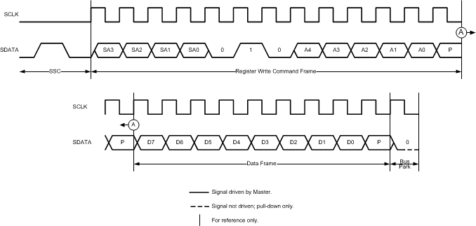
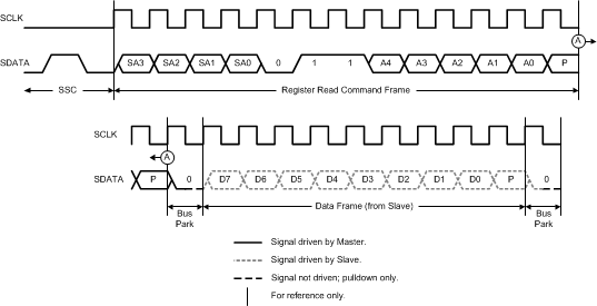
7.5.2 Supported Command Sequences
 Figure 19. Register 0 Write
 Figure 20. Register Write
 Figure 21. Register Read
7.5.3 Device Enumeration
The interface component recognizes broadcast Slave Address (SID) of 0000b and is configured, via internal interface signals, with a Unique SID address (USID) and a Group SID address (GSID). The USID is set to 0101b and GSID set to 0000b. The register-set component will typically set the USID to a fixed value; however, it is also possible to construct a register-set component that allows the USID to be programmed via the RFFE bus.
7.5.4 I/O
This RFFE interface supports a 1.8-V VIO supply level. A power-on reset circuit will be included that resets the RFFE interface and register-set components when VIO is removed.
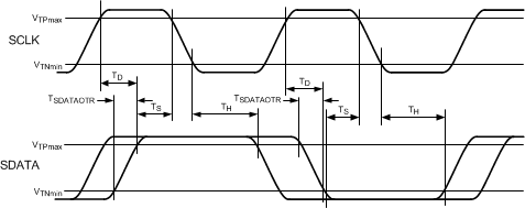
7.5.5 Control Interface Timing Parameters
 Figure 22. Clock Timing
 Figure 23. Setup And Hold Timing