ZHCSBI0C March 2013 – October 2014 LM3279
PRODUCTION DATA.
- 1 特性
- 2 应用
- 3 说明
- 4 修订历史记录
- 5 Pin Configuration and Functions
- 6 Specifications
- 7 Detailed Description
- 8 Application and Implementation
- 9 Power Supply Recommendations
- 10Layout
- 11器件和文档支持
- 12机械、封装和可订购信息
6 Specifications
6.1 Absolute Maximum Ratings
over operating free-air temperature range (unless otherwise noted) (1)(2)| MIN | MAX | UNIT | ||
|---|---|---|---|---|
| PVIN, VOUT to GND | −0.2 | 6 | V | |
| PGND to SGND, GND | PGND −0.2 | 0.2 | ||
| VIO, SDATA, SCLK, EN, VCON, GPO1/GPO0 to SGND, GND | −0.2 | 6 | ||
| FB to PGND | −0.2 | 6 | ||
| SW1, SW2 | (PGND −0.2V) | 6 | ||
| Continuous power dissipation (3) | Internally limited | |||
| Maximum operating junction temperature (TJ-MAX) | 150 | °C | ||
| Maximum lead temperature (soldering) | See (4) | |||
(1) Stresses beyond those listed under Absolute Maximum Ratings may cause permanent damage to the device. These are stress ratings only, which do not imply functional operation of the device at these or any other conditions beyond those indicated under Recommended Operating Conditions. Exposure to absolute-maximum-rated conditions for extended periods may affect device reliability.
(2) All voltages are with respect to the potential at the GND pins.
(3) Internal thermal shutdown circuitry protects the device from permanent damage. Thermal shutdown engages at TJ = 150°C (typ.) and disengages at TJ = 125°C (typ.).
(4) For detailed soldering specifications and information, please refer to Texas Instruments Application Note 1112: DSBGA Wafer Level Chip Scale Package (SNVA009).
6.2 Handling Ratings
| MIN | MAX | UNIT | |||
|---|---|---|---|---|---|
| Tstg | Storage temperature range | –45 | 150 | °C | |
| V(ESD) | Electrostatic discharge | Human body model (HBM), per ANSI/ESDA/JEDEC JS-001, all pins(1) | 0 | 1000 | V |
(1) JEDEC document JEP155 states that 500-V HBM allows safe manufacturing with a standard ESD control process.
6.3 Recommended Operating Conditions
over operating free-air temperature range (unless otherwise noted) (1)(2)| MIN | NOM | MAX | UNIT | ||
|---|---|---|---|---|---|
| Input voltage | 2.7 | 5.5 | V | ||
| Output voltage (digital control) | 0.4 | 4.212 | |||
| Recommended current load | 0 | 1000 | mA | ||
| Operating ambient temperature (TA)(3) | –30 | 85 | °C | ||
(1) Stresses beyond those listed under Absolute Maximum Ratings may cause permanent damage to the device. These are stress ratings only, which do not imply functional operation of the device at these or any other conditions beyond those indicated under Recommended Operating Conditions. Exposure to absolute-maximum-rated conditions for extended periods may affect device reliability.
(2) All voltages are with respect to the potential at the GND pins.
(3) In applications where high power dissipation and/or poor package thermal resistance is present, the maximum ambient temperature may have to be de-rated. Maximum ambient temperature (TA-MAX) is dependent on the maximum operating junction temperature (TJ-MAX-OP = 125°C), the maximum power dissipation of the device in the application (PD-MAX), and the junction-to ambient thermal resistance of the part/package in the application (RθJA), as given by the following equation: TA-MAX = TJ-MAX-OP – (RθJA × PD-MAX).
6.4 Thermal Information
| THERMAL METRIC(1) | DSBGA | UNIT | |
|---|---|---|---|
| YZR | |||
| 16 PINS | |||
| RθJA | Junction-to-ambient thermal resistance | 70.1 | °C/W |
| RθJC(top) | Junction-to-case (top) thermal resistance | 14.4 | |
| RθJB | Junction-to-board thermal resistance | 10 | |
| ψJT | Junction-to-top characterization parameter | 1.7 | |
| ψJB | Junction-to-board characterization parameter | 10 | |
| RθJC(bot) | Junction-to-case (bottom) thermal resistance | N/A | |
(1) For more information about traditional and new thermal metrics, see the IC Package Thermal Metrics application report, SPRA953.
6.5 Electrical Characteristics(1)
Limits are for TA = TJ = 25°C, and specifications apply to the LM3279 Typical Application Circuits with: PVIN = 3.8 V, VIO or EN = 1.8 V, unless otherwise specified.| PARAMETER | TEST CONDITIONS | MIN | TYP | MAX | UNIT | |
|---|---|---|---|---|---|---|
| VFB,MIN | Minimum FB voltage | VSET = 0Bh | 0.35 | 0.40 | 0.45 | V |
| VCON = 0.167 V | 0.43 | 0.5 | 0.570 | |||
| VFB,MAX | Maximum FB voltage | VSET = 75h | 4.122 | 4.212 | 4.302 | |
| VCON = 1.4 V | 4.11 | 4.2 | 4.29 | |||
| IQ_PWM | DC bias current in PVIN, SVIN | No switching (2) FB = HIGH Max limits = −30°C ≤ TJ = TA ≤ 85°C |
1.4 | 2 | mA | |
| ISHDN | Shutdown supply current | VIO = EN = 0 V, VCON = 0 V, SW1 = SW2 = VOUT = 0 V Max limits = −30°C ≤ TJ = TA ≤ 85°C |
0.2 | 2 | µA | |
| IQ STBY | Standby supply current | VIO = 1.8 V, VSET_CTRL = 02h, SW1 = SW2 = VOUT = 0 V |
1.2 | mA | ||
| ILIM_L | Input current limit (large) | Open Loop (3) VCON = 1.2 V | 1500 | 1700 | mA | |
| ILIM_S | Input current limit (small) | Open Loop (3) VCON = 0.2 V | 700 | 850 | ||
| ƒOSC_PWM | Internal oscillator frequency | PWM Min and Max limits = −30°C ≤ TJ = TA ≤ 85°C |
2.1 | 2.4 | 2.7 | MHz |
| fSCLK | SCLK clock frequency | 0.032 | 26 | |||
| IVIO-IN | VIO voltage average input current | VIO = 1.8 V, Average during 26-MHz write | 1.25 | mA | ||
| IIL | ISDATA | VIN = 0.2*VIO | −2 | 1 | µA | |
| ISCLK | −1 | 1 | ||||
| IIH | ISDATA | VIN = 0.8*VIO | −2 | 10 | ||
| ISCLK | −1 | 10 | ||||
| VIH | Input high-level threshold EN, GPO0, GPO1 | Min and Max limits = −30°C ≤ TJ = TA ≤ 85°C | 1.2 | V | ||
| VIL | Input low-level threshold EN, GPO0, GPO1 | 0.6 | ||||
| VIH-SDATA, SCLK | Input high-level threshold SDATA, SCLK | 0.4*VIO | 0.7*VIO | V | ||
| VIL-SDATA, SCLK | Input low-level threshold SDATA, SCLK | 0.3*VIO | 0.6*VIO | |||
| VOH-SDATA | Output high-level threshold SDATA | ISDATA = −2 mA | 0.8*VIO | VIO + 0.01 | ||
| VOL-SDATA | Output low-level threshold SDATA | ISDATA = 2 mA | 0.2*VIO | |||
| VOH-GPO | Output high-level threshold GPO | IOUT = ±200 µA | VIO−0.15V | VIO+0.1V | ||
| VOL-GPO | Output low-level threshold GPO | IOUT = ±200 µA | −0.4 | 0.3 | V | |
| VSET-LSB | Output voltage LSB | VSET_CTRL = 40h to 41h | 36 | mV | ||
| IEN | EN pin pulldown current | VIO = 0 V | 5 | 10 | µA | |
| Gain | Internal gain (4) | 0.167 V ≤ VCON ≤ 1.4 V | 3 | V/V | ||
| ICON | VCON pin input leakage | EN = 3.8 V | –1 | 1 | µA | |
| IOUT_LEAKAGE | Leakage into VOUT pin of the buck-boost | EN = 0, VOUT ≤ 4.2 V, VBATT ≤ 5.5 V Max limits = −30°C ≤ TJ = TA ≤ 85°C |
5 | |||
(1) Min and Max limits are specified by design, test, or statistical analysis.
(2) IQ specified here is when the part is not switching.
(3) The parameters in the electrical characteristics table are tested under open loop conditions at PVIN = 3.8 V. For performance over the input voltage range and closed loop results refer to the datasheet curves.
(4) When using analog control (EN = HIGH) to calculate VOUT, use the following equation: VOUT = VCON × 3.
6.6 System Characteristics
The following spec table entries are specified by design and verifications, providing the component values in the typical application circuits are used: L = 1.5 µH, DFE201610C-1R5M (2016)/TOKO; CIN and COUT each = 10 µF 6.3 V, C105A106MQ5NUNC (0402)/Samsung; PA decoupling cap emulation = 0.47 µF, GRM033R60J474ME90 (0201)/Murata. These parameters are not verified by production testing. Typical limits are TA = 25°C. Min and Max limits apply over the full ambient temperature range (−30°C ≤ TA ≤ 85°C) and over the VIN range = 2.7 V to 5.5 V, unless otherwise specified.6.7 System Characteristics Recommended Capacitance Specifications
| BUS | MIN (µF) | TYP (µF) | MAX (µF) |
|---|---|---|---|
| VBATT | 4.7 | 10 | — |
| VOUT | 3.0 | 13 |
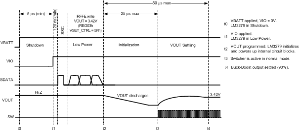 Figure 1. Cold Power-Up
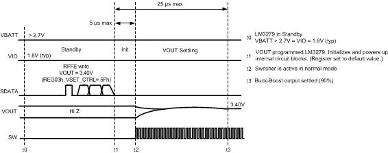 Figure 2. Standby To Active
6.8 Typical Performance Characteristics
(PVIN = EN = 3.6 V and TA = 25°C, unless otherwise noted)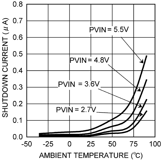
| VCON = VOUT = SW1 = SW2 = EN = 0 V | ||
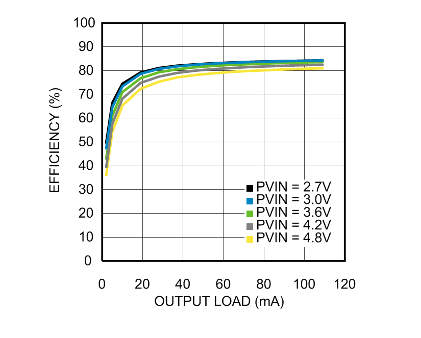
| VOUT = 1 V | ||
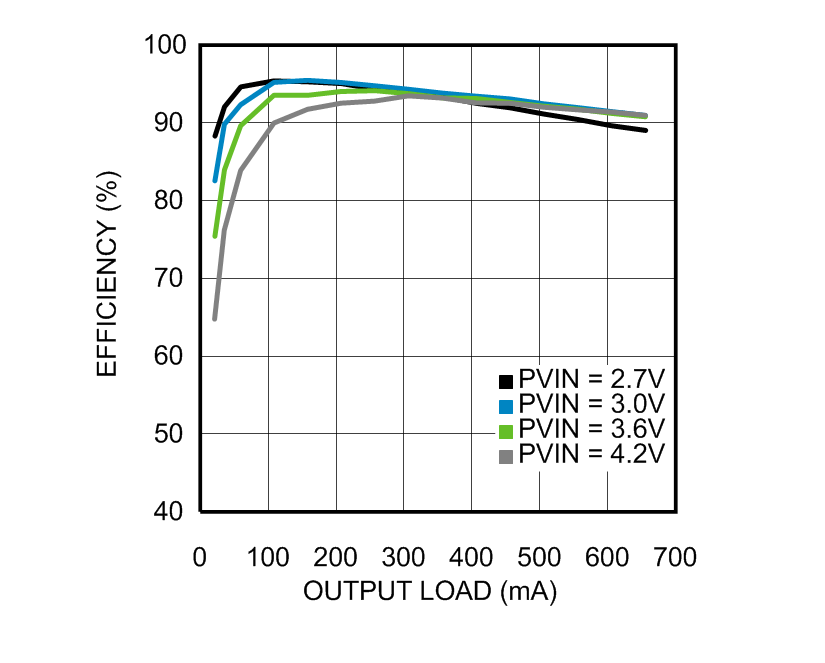
| VOUT = 2.4 V | ||
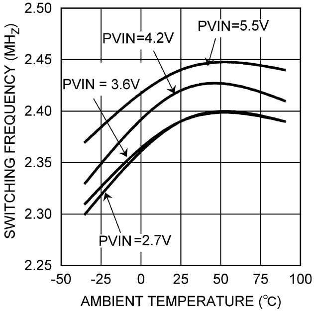
| VOUT = 3.5 V | IOUT = 300 mA | |
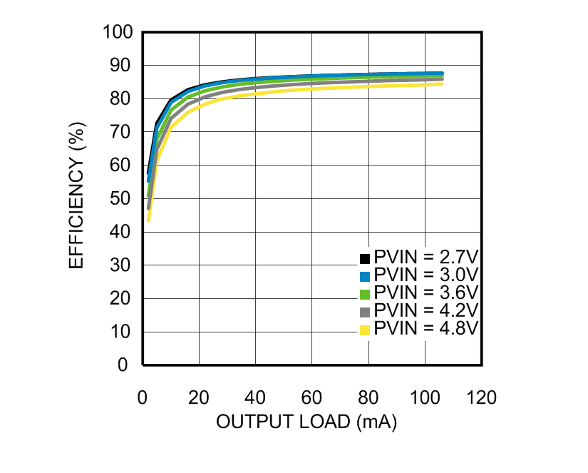
| VOUT = 1.4 V | ||
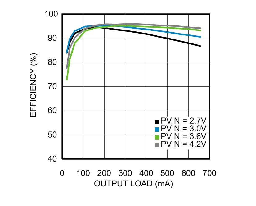
| VOUT = 3.6 V | ||
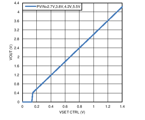
| No Load, RFFE Digital Control Mode | ||
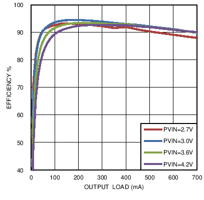
| VOUT = 2.5 V | ||
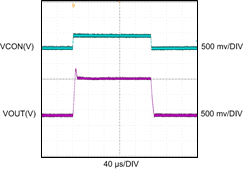
| VOUT = 0.8 ↔ 2 V | PVIN = 3.8 V | RLOAD = 20 Ω |
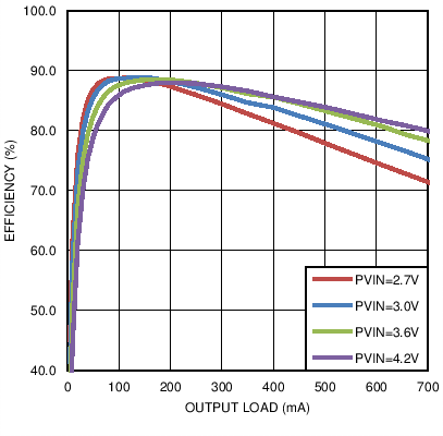
| VOUT = 1.5 V | ||
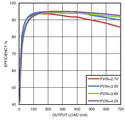
| VOUT = 3.4 V | ||
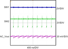
| VOUT = 3.45 V | PVIN = 3.37 V | LOAD = 500 mA |
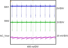
| VOUT = 3.6 V | PVIN = 3.8 V | LOAD = 600 mA |
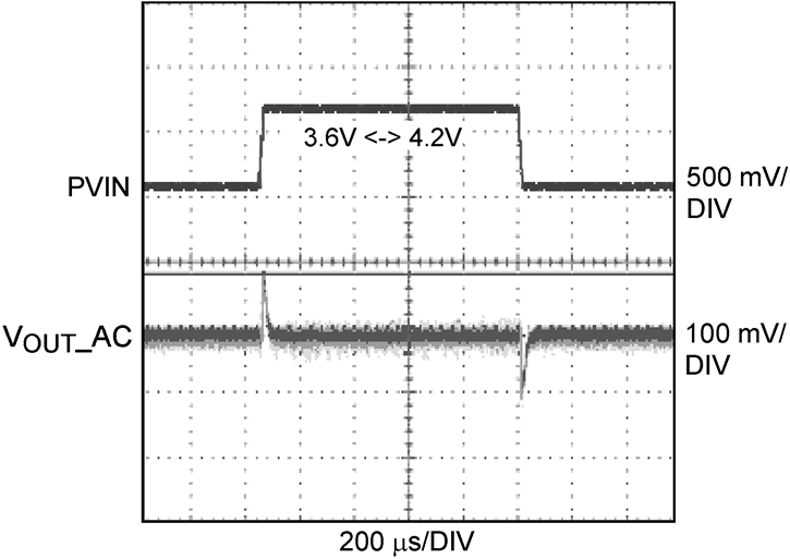
| VOUT = 3 V | PVIN Step = 3.6 V ↔ 4.2 V | LOAD = 3200 mA |
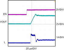
| VOUT = 3.45 V | PVIN = 3.6 V | LOAD = 350 mA |
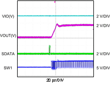
| VOUT = 3.5 V | PVIN = 4.2 V | VIO = 1.8 V |
| VSET_CTRL = 0x5F |