SBOS160A November 1993 – January 2015 ISO122
PRODUCTION DATA.
- 1 Features
- 2 Applications
- 3 Description
- 4 Simplified Schematic
- 5 Revision History
- 6 Pin Configuration and Functions
- 7 Specifications
- 8 Detailed Description
-
9 Application and Implementation
- 9.1 Application Information
- 9.2 Typical Application
- 10Power Supply Recommendations
- 11Layout
- 12Device and Documentation Support
- 13Mechanical, Packaging, and Orderable Information
7 Specifications
7.1 Absolute Maximum Ratings
over operating free-air temperature range (unless otherwise noted) (1)| MIN | MAX | UNIT | |
|---|---|---|---|
| Supply voltage | ±18 | V | |
| VIN | 100 | V | |
| Continuous isolation voltage | 1500 | Vrms | |
| Junction temperature | 150 | °C | |
| Output short to common | Continuous | ||
| Storage temperature, Tstg | –40 | 125 | °C |
(1) Stresses beyond those listed under Absolute Maximum Ratings may cause permanent damage to the device. These are stress ratings only, which do not imply functional operation of the device at these or any other conditions beyond those indicated under Recommended Operating Conditions. Exposure to absolute-maximum-rated conditions for extended periods may affect device reliability.
7.2 ESD Ratings
| VALUE | UNIT | |||
|---|---|---|---|---|
| V(ESD) | Electrostatic discharge | Human body model (HBM), per ANSI/ESDA/JEDEC JS-001(1) | ±1000 | V |
| Charged-device model (CDM), per JEDEC specification JESD22-C101(2) | ±500 | |||
(1) JEDEC document JEP155 states that 500-V HBM allows safe manufacturing with a standard ESD control process.
(2) JEDEC document JEP157 states that 250-V CDM allows safe manufacturing with a standard ESD control process.
7.3 Recommended Operating Conditions
over operating free-air temperature range (unless otherwise noted)| MIN | NOM | MAX | UNIT | ||
|---|---|---|---|---|---|
| TA | –25 | 85 | °C | ||
| +VS1 | 15 | ||||
| -VS1 | –15 | ||||
| +VS2 | 15 | ||||
| -VS2 | –15 | ||||
| VIN | ±10 | ||||
7.4 Thermal Information
| THERMAL METRIC(1) | ISO122 | UNIT | ||
|---|---|---|---|---|
| NVF (PDIP) | DVA (SOIC) | |||
| 16 PINS | 28 PINS | |||
| RθJA | Junction-to-ambient thermal resistance | 51.0 | 79.8 | °C/W |
| RθJC(top) | Junction-to-case (top) thermal resistance | 32.4 | 32.9 | |
| RθJB | Junction-to-board thermal resistance | 29.5 | 42.2 | |
| ψJT | Junction-to-top characterization parameter | 10.4 | 6.6 | |
| ψJB | Junction-to-board characterization parameter | 29.0 | 40.9 | |
(1) For more information about traditional and new thermal metrics, see the IC Package Thermal Metrics application report, SPRA953.
7.5 Electrical Characteristics
At TA = +25°C , VS1 = VS2 = ±15 V, and RL = 2 kΩ, unless otherwise noted.| PARAMETER | TEST CONDITIONS | ISO122P/U | ISO122JP/JU | UNIT | |||||
|---|---|---|---|---|---|---|---|---|---|
| MIN | TYP | MAX | MIN | TYP | MAX | ||||
| ISOLATION | |||||||||
| Voltage rated continuous ac 60Hz | 1500 | 1500 | Vac | ||||||
| 100% Test(1) | 1s, 5pc PD | 2400 | 2400 | Vac | |||||
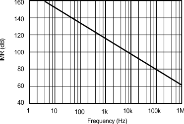
| Isolation Mode Rejection | 60Hz | 140 | 140 | dB | |||||
| Barrier Impedance | 1014 || 2 | 1014 || 2 | Ω || pF | ||||||
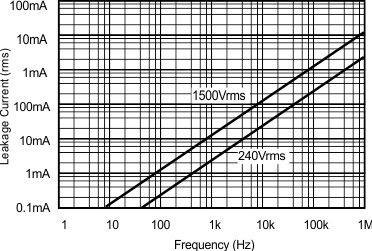
| Leakage Current at 60Hz | VISO = 240Vrms | 0.18 | 0.5 | 0.18 | 0.5 | µArms | |||
| GAIN | |||||||||
| Nominal Gain | VO = ±10V | 1 | 1 | V/V | |||||
| Gain Error | ±0.05 | ±0.50 | ±0.05 | ±0.50 | %FSR | ||||
| Gain vs Temperature | ±10 | ±10 | ppm/°C | ||||||
| Nonlinearity(2) | ±0.016 | ±0.020 | ±0.025 | ±0.050 | %FSR | ||||
| INPUT OFFSET VOLTAGE | |||||||||
| Initial Offset | ±20 | ±50 | ±20 | ±50 | mV | ||||
| vs Temperature | ±200 | ±200 | µV/°C | ||||||
| vs Supply | ±2 | ±2 | mV/V | ||||||
| Noise | 4 | µV/√Hz | |||||||
| INPUT | |||||||||
| Voltage Range | ±10 | ±12.5 | ±10 | ±12.5 | V | ||||
| Resistance | 200 | 200 | kΩ | ||||||
| OUTPUT | |||||||||
| Voltage Range | ±10 | ±12.5 | ±10 | ±12.5 | V | ||||
| Current Drive | ±5 | ±15 | ±5 | ±15 | mA | ||||
| Capacitive Load Drive | 0.1 | 0.1 | µF | ||||||
| Ripple Voltage(3) | 20 | 20 | mVp-p | ||||||
| FREQUENCY RESPONSE | |||||||||
| Small-Signal Bandwidth | 50 | 50 | kHz | ||||||
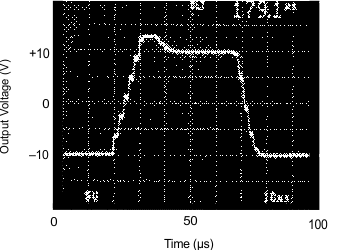
| Slew Rate | 2 | 2 | V/µs | ||||||
| Settling Time 0.10% | VO = ±10V | 50 | 50 | µs | |||||
| Settling Time 0.01% | 350 | 350 | µs | ||||||
| Overload Recovery Time | 150 | 150 | µs | ||||||
| POWER SUPPLIES | |||||||||
| Rated Voltage | ±15 | ±15 | V | ||||||
| Voltage Range | ±4.5 | ±18 | ±4.5 | ±18 | V | ||||
| VS1 | Quiescent Current | ±5 | ±7 | ±5 | ±7 | mA | |||
| VS2 | ±5.5 | ±7 | ±5.5 | ±7 | |||||
| TEMPERATURE RANGE | |||||||||
| Specification | –25 | 85 | –25 | 85 | °C | ||||
| Operating | –25 | 85 | –25 | 85 | °C | ||||
| Storage | –40 | 125 | –40 | 125 | °C | ||||
| θJA | Thermal Resistance | 100 | 100 | °C/W | |||||
| θJC | 65 | 65 | °C/W | ||||||
(1) Tested at 1.6 X rated, fail on 5pC partial discharge.
(2) Nonlinearity is the peak deviation of the output voltage from the best-fit straight line. It is expressed as the ratio of deviation to FSR.
(3) Ripple frequency is at carrier frequency (500kHz).
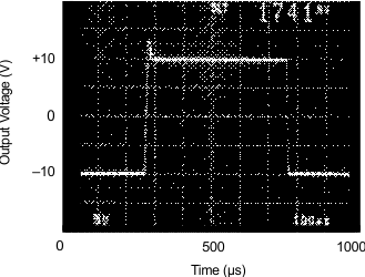
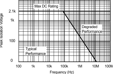
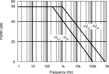
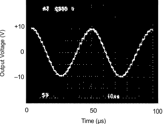
7.6 Typical Characteristics
At TA = +25°C, and VS = ±15 V, unless otherwise noted.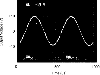
| f = 2kHz | ||
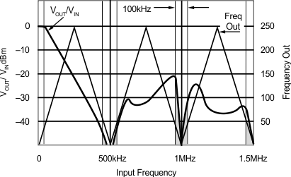
| NOTE: Shaded area shows aliasing frequencies that cannot be removed by a low-pass filter at the output. | ||||
| f = 20kHz | ||