SBOS160A November 1993 – January 2015 ISO122
PRODUCTION DATA.
- 1 Features
- 2 Applications
- 3 Description
- 4 Simplified Schematic
- 5 Revision History
- 6 Pin Configuration and Functions
- 7 Specifications
- 8 Detailed Description
-
9 Application and Implementation
- 9.1 Application Information
- 9.2 Typical Application
- 10Power Supply Recommendations
- 11Layout
- 12Device and Documentation Support
- 13Mechanical, Packaging, and Orderable Information
10 Power Supply Recommendations
10.1 Signal and Supply Connections
Each power-supply pin should be bypassed with 1-µF tantalum capacitors located as close to the amplifier as possible. The internal frequency of the modulator/demodulator is set at 500 kHz by an internal oscillator. Therefore, if it is desired to minimize any feedthrough noise (beat frequencies) from a DC-DC converter, use a π filter on the supplies (see Figure 24). The ISO122 output has a 500-kHz ripple of 20 mV, which can be removed with a simple 2-pole low-pass filter with a 100-kHz cutoff using a low-cost op amp (see Figure 10).
The input to the modulator is a current (set by the 200-kΩ integrator input resistor) that makes it possible to have an input voltage greater than the input supplies, as long as the output supply is at least ±15 V. It is therefore possible, when using an unregulated DC-DC converter, to minimize PSR related output errors with ±5-V voltage regulators on the isolated side and still get the full ±10V input and output swing.
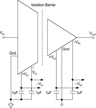 Figure 24. Basic Signal and Power Connections