SBOS160A November 1993 – January 2015 ISO122
PRODUCTION DATA.
- 1 Features
- 2 Applications
- 3 Description
- 4 Simplified Schematic
- 5 Revision History
- 6 Pin Configuration and Functions
- 7 Specifications
- 8 Detailed Description
-
9 Application and Implementation
- 9.1 Application Information
- 9.2 Typical Application
- 10Power Supply Recommendations
- 11Layout
- 12Device and Documentation Support
- 13Mechanical, Packaging, and Orderable Information
8 Detailed Description
8.1 Overview
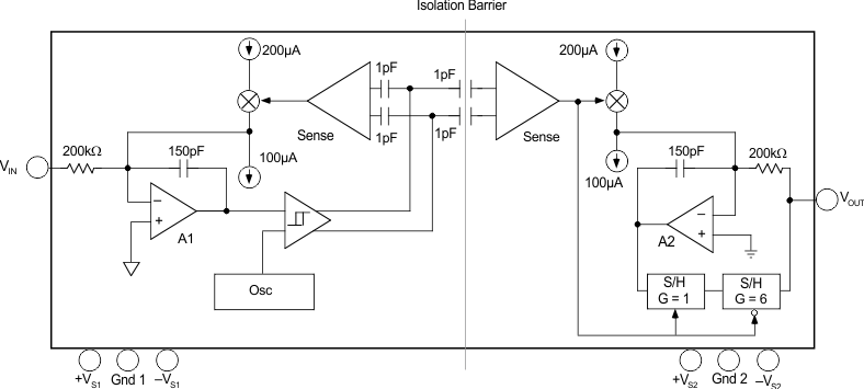
The ISO122 isolation amplifier uses an input and an output section galvanically isolated by matched 1-pF isolating capacitors built into the plastic package. The input is duty-cycle modulated and transmitted digitally across the barrier. The output section receives the modulated signal, converts it back to an analog voltage and removes the ripple component inherent in the demodulation. Input and output sections are fabricated, then laser trimmed for exceptional circuitry matching common to the input and output sections. The sections are then mounted on opposite ends of the package with the isolating capacitors mounted between the two sections. The ISO122 contains 250 transistors.
8.1.1 Modulator
An input amplifier (A1, Functional Block Diagram) integrates the difference between the input current (VIN/200 kΩ) and a switched ±100-mA current source. This current source is implemented by a switchable 200-mA source and a fixed 100-µA current sink. To understand the basic operation of the modulator, assume that VIN = 0 V. The integrator will ramp in one direction until the comparator threshold is exceeded. The comparator and sense amp will force the current source to switch; the resultant signal is a triangular waveform with a 50% duty cycle. The internal oscillator forces the current source to switch at 500 kHz. The resultant capacitor drive is a complementary duty-cycle modulation square wave.
8.1.2 Demodulator
The sense amplifier detects the signal transitions across the capacitive barrier and drives a switched current source into integrator A2. The output stage balances the duty-cycle modulated current against the feedback current through the 200 kW feedback resistor, resulting in an average value at the VOUT pin equal to VIN. The sample and hold amplifiers in the output feedback loop serve to remove undesired ripple voltages inherent in the demodulation process.
8.2 Functional Block Diagram
8.3 Feature Description
8.3.1 Isolation Amplifier
The ISO122 is a precision analog isolation amplifier. The input signal is transmitted digitally across a high-voltage differential capacitive barrier. With digital modulation the barrier characteristics do affect signal integrity, resulting in excellent reliability and high-frequency transient immunity.
8.4 Device Functional Modes
The ISO122 does not have any additional functional modes.