SBOS160A November 1993 – January 2015 ISO122
PRODUCTION DATA.
- 1 Features
- 2 Applications
- 3 Description
- 4 Simplified Schematic
- 5 Revision History
- 6 Pin Configuration and Functions
- 7 Specifications
- 8 Detailed Description
-
9 Application and Implementation
- 9.1 Application Information
- 9.2 Typical Application
- 10Power Supply Recommendations
- 11Layout
- 12Device and Documentation Support
- 13Mechanical, Packaging, and Orderable Information
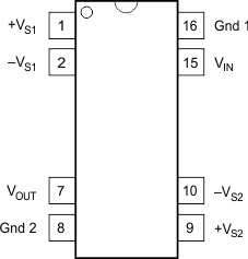
6 Pin Configuration and Functions
NVF Package
16 Pins PDIP
Top View
DVA Package
28 Pins SOIC
Top View
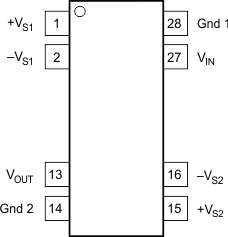
Pin Functions
| PIN | I/O | DESCRIPTION | ||
|---|---|---|---|---|
| NAME | PDIP | SOIC | ||
| GND | 8 | 14 | - | Low-side ground reference |
| GND | 16 | 28 | - | High-side ground reference |
| VIN | 15 | 27 | I | High-side analog input |
| VOUT | 7 | 13 | O | Low-side analog output |
| +VS1 | 1 | 1 | - | High-side positive analog supply |
| -VS1 | 2 | 2 | - | High-side negative analog supply |
| +VS2 | 9 | 15 | - | Low-side positive analog supply |
| -VS2 | 10 | 16 | - | Low-side negative analog supply |