ZHCSHW8B March 2018 – July 2018 INA1620
PRODUCTION DATA.
- 1 特性
- 2 应用
- 3 说明
- 4 修订历史记录
- 5 Pin Configuration and Functions
- 6 Specifications
- 7 Detailed Description
- 8 Application and Implementation
- 9 Power Supply Recommendations
- 10Layout
- 11器件和文档支持
- 12机械、封装和可订购信息
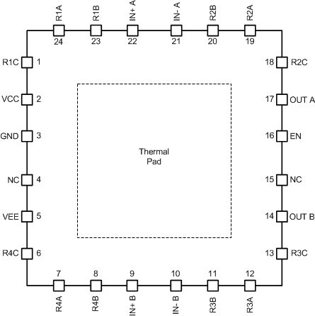
5 Pin Configuration and Functions
RTW Package
24-Pin QFN
Top View

Pin Functions
| PIN | I/O | DESCRIPTION | |
|---|---|---|---|
| NAME | NO. | ||
| GND | 3 | — | Connect to ground |
| EN | 16 | I | Shutdown (logic low), enable (logic high) |
| IN+ A | 22 | I | Noninverting input, channel A |
| IN- A | 21 | I | Inverting input, channel A |
| IN+ B | 9 | I | Noninverting input, channel B |
| IN- B | 10 | I | Inverting input, channel B |
| NC | 4 | — | No internal connection |
| NC | 15 | — | No internal connection |
| OUT A | 17 | O | Output, channel A |
| OUT B | 14 | O | Output, channel B |
| R1A | 24 | — | Resistor pair 1, end point A |
| R1B | 23 | — | Resistor pair 1, center point |
| R1C | 1 | — | Resistor pair 1, end point C |
| R2A | 19 | — | Resistor pair 2, end point A |
| R2B | 20 | — | Resistor pair 2, center point |
| R2C | 18 | — | Resistor pair 2, end point C |
| R3A | 12 | — | Resistor pair 3, end point A |
| R3B | 11 | — | Resistor pair 3, center point |
| R3C | 13 | — | Resistor pair 3, end point C |
| R4A | 7 | — | Resistor pair 4, end point A |
| R4B | 8 | — | Resistor pair 4, center point |
| R4C | 6 | — | Resistor pair 4, end point C |
| V+ | 2 | — | Positive (highest) power supply |
| V– | 5 | — | Negative (lowest) power supply |
| Thermal pad | Exposed thermal die pad on underside; connect thermal die pad to V–. | ||