ZHCSHW8B March   2018  – July 2018 INA1620

PRODUCTION DATA.  

  1. 特性
  2. 应用
  3. 说明
    1.     Device Images
      1.      INA1620 简化内部原理图
      2.      快速傅立叶变换 (FFT):1kHz、32Ω 负载、50mW
  4. 修订历史记录
  5. Pin Configuration and Functions
    1.     Pin Functions
  6. Specifications
    1. 6.1 Absolute Maximum Ratings
    2. 6.2 ESD Ratings
    3. 6.3 Recommended Operating Conditions
    4. 6.4 Thermal Information
    5. 6.5 Electrical Characteristics:
    6. 6.6 Typical Characteristics
  7. Detailed Description
    1. 7.1 Overview
    2. 7.2 Functional Block Diagram
    3. 7.3 Feature Description
      1. 7.3.1 Matched Thin-Film Resistor Pairs
      2. 7.3.2 Power Dissipation
      3. 7.3.3 Thermal Shutdown
      4. 7.3.4 EN Pin
      5. 7.3.5 GND Pin
      6. 7.3.6 Input Protection
    4. 7.4 Device Functional Modes
      1. 7.4.1 Shutdown Mode
      2. 7.4.2 Output Transients During Power Up and Power Down
  8. Application and Implementation
    1. 8.1 Application Information
      1. 8.1.1 Noise Performance
      2. 8.1.2 Resistor Tolerance
      3. 8.1.3 EMI Rejection
      4. 8.1.4 EMIRR +IN Test Configuration
    2. 8.2 Typical Application
      1. 8.2.1 Design Requirements
      2. 8.2.2 Detailed Design Procedure
      3. 8.2.3 Application Curves
    3. 8.3 Other Application Examples
      1. 8.3.1 Preamplifier for Professional Microphones
  9. Power Supply Recommendations
  10. 10Layout
    1. 10.1 Layout Guidelines
    2. 10.2 Layout Example
  11. 11器件和文档支持
    1. 11.1 器件支持
      1. 11.1.1 开发支持
        1. 11.1.1.1 TINA-TI(免费软件下载)
        2. 11.1.1.2 TI 高精度设计
    2. 11.2 文档支持
      1. 11.2.1 相关文档
    3. 11.3 接收文档更新通知
    4. 11.4 社区资源
    5. 11.5 商标
    6. 11.6 静电放电警告
    7. 11.7 术语表
  12. 12机械、封装和可订购信息

封装选项

机械数据 (封装 | 引脚)
散热焊盘机械数据 (封装 | 引脚)
订购信息

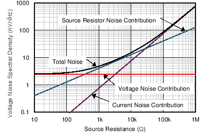
Noise Performance

Figure 51 shows the total circuit noise for varying source impedances with the op amp in a unity-gain configuration (no feedback resistor network, and therefore no additional noise contributions).

The INA1620 is shown with total circuit noise calculated. The op amp contributes both a voltage noise component and a current noise component. The voltage noise is commonly modeled as a time-varying component of the offset voltage. The current noise is modeled as the time-varying component of the input bias current, and reacts with the source resistance to create a voltage component of noise. Therefore, the lowest noise op amp for a given application depends on the source impedance. For low source impedance, current noise is negligible, and voltage noise generally dominates. The low voltage and current noise of the INA1620 internal op amps make the device an excellent choice for use in applications where the source impedance is less than 10 kΩ as shown in Figure 51.
INA1620 C302_SBOS727.pngFigure 51. Noise Performance of the INA1620 Internal Amplifiers