ZHCSHW8B March 2018 – July 2018 INA1620
PRODUCTION DATA.
- 1 特性
- 2 应用
- 3 说明
- 4 修订历史记录
- 5 Pin Configuration and Functions
- 6 Specifications
- 7 Detailed Description
- 8 Application and Implementation
- 9 Power Supply Recommendations
- 10Layout
- 11器件和文档支持
- 12机械、封装和可订购信息
8.2.2 Detailed Design Procedure
Figure 55 shows a schematic of a headphone amplifier circuit for voltage output DACs. An op amp is configured as a difference amplifier that converts the differential output voltage to single-ended.
The gain of the difference amplifier in Figure 55 is determined by the resistor values, and includes the output impedance of the DAC. For R2 = R4 and R1 = R3, the output voltage of the headphone amplifier circuit is shown in Equation 6:

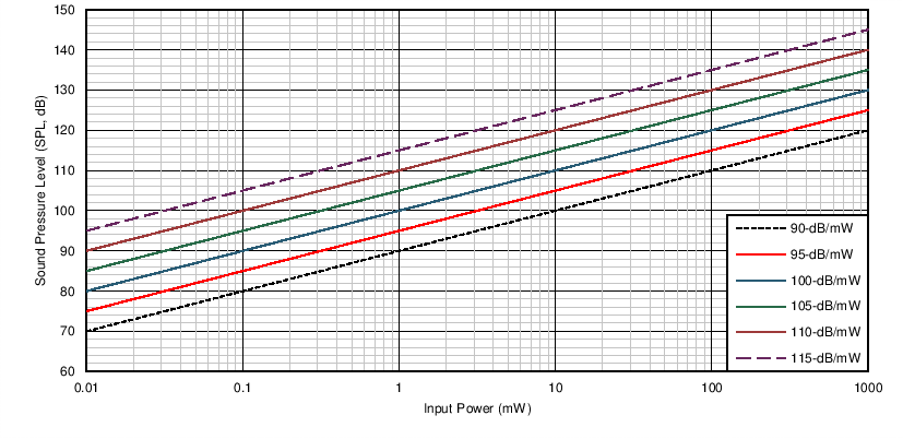
The output voltage required for headphones depends on the headphone impedance, as well as the headphone efficiency (η), a measure of the sound pressure level (SPL, measured in dB) for a certain input power level (typically given at 1 mW). The headphone SPL at other power levels is calculated using Equation 7:

where
- η = efficiency
- PIN = input power to the headphones
Figure 56 shows the input power required to produce certain SPLs for different headphone efficiencies. Typically, over-the-ear style headphones have lower efficiencies than in-ear types with 95 dB/mW being a common value.
 Figure 56. Sound Pressure Level vs Input Power for Headphones of Various Efficiencies
 In-ear headphones can have efficiencies of 115 dB/mW or greater, and therefore have much lower power requirements. The output power goal for this design is 150 mW — sufficient power to produce extremely loud sound pressure levels in a wide range of headphones. A 32-Ω headphone impedance is used for this requirement because 32 Ω is a very common value in headphones for portable applications. Equation 8 shows the voltage required for 32-Ω headphones:

Capacitors C1 and C2 limit the bandwidth of the circuit to prevent the unnecessary amplification of interfering signals. The maximum value of these capacitors is determined by the limitations on frequency response magnitude deviation detailed in the Design Requirements section. C1 and C2 combine with resistors R2 and R4 to form a pole, as shown in Equation 9:

Calculate the minimum pole frequency allowable to meet the magnitude deviation requirements using Equation 10:

where
- G represents the gain in decimal for a –0.01-dB deviation at 20 kHz.
Use Equation 11 to calculate the upper limit for the value of C1 and C2 in order to meet the goal for minimal magnitude deviation at 20 kHz.

For this design, 100-pF capacitors were used because they meet the design requirements for amplitude deviation in the audio bandwidth.