ZHCSHW8B March   2018  – July 2018 INA1620

PRODUCTION DATA.  

  1. 特性
  2. 应用
  3. 说明
    1.     Device Images
      1.      INA1620 简化内部原理图
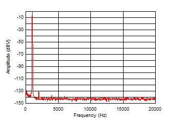
      2.      快速傅立叶变换 (FFT):1kHz、32Ω 负载、50mW
  4. 修订历史记录
  5. Pin Configuration and Functions
    1.     Pin Functions
  6. Specifications
    1. 6.1 Absolute Maximum Ratings
    2. 6.2 ESD Ratings
    3. 6.3 Recommended Operating Conditions
    4. 6.4 Thermal Information
    5. 6.5 Electrical Characteristics:
    6. 6.6 Typical Characteristics
  7. Detailed Description
    1. 7.1 Overview
    2. 7.2 Functional Block Diagram
    3. 7.3 Feature Description
      1. 7.3.1 Matched Thin-Film Resistor Pairs
      2. 7.3.2 Power Dissipation
      3. 7.3.3 Thermal Shutdown
      4. 7.3.4 EN Pin
      5. 7.3.5 GND Pin
      6. 7.3.6 Input Protection
    4. 7.4 Device Functional Modes
      1. 7.4.1 Shutdown Mode
      2. 7.4.2 Output Transients During Power Up and Power Down
  8. Application and Implementation
    1. 8.1 Application Information
      1. 8.1.1 Noise Performance
      2. 8.1.2 Resistor Tolerance
      3. 8.1.3 EMI Rejection
      4. 8.1.4 EMIRR +IN Test Configuration
    2. 8.2 Typical Application
      1. 8.2.1 Design Requirements
      2. 8.2.2 Detailed Design Procedure
      3. 8.2.3 Application Curves
    3. 8.3 Other Application Examples
      1. 8.3.1 Preamplifier for Professional Microphones
  9. Power Supply Recommendations
  10. 10Layout
    1. 10.1 Layout Guidelines
    2. 10.2 Layout Example
  11. 11器件和文档支持
    1. 11.1 器件支持
      1. 11.1.1 开发支持
        1. 11.1.1.1 TINA-TI(免费软件下载)
        2. 11.1.1.2 TI 高精度设计
    2. 11.2 文档支持
      1. 11.2.1 相关文档
    3. 11.3 接收文档更新通知
    4. 11.4 社区资源
    5. 11.5 商标
    6. 11.6 静电放电警告
    7. 11.7 术语表
  12. 12机械、封装和可订购信息

封装选项

机械数据 (封装 | 引脚)
散热焊盘机械数据 (封装 | 引脚)
订购信息

Application Curves

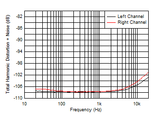
Figure 57 shows the maximum output voltage achievable for a 32-Ω load before the onset of clipping (±5-V supplies), indicated by a sharp increase in distortion. As more current is delivered by the output transistors of an amplifier, additional distortion is produced. At low frequencies, this distortion is corrected by the feedback loop of the amplifier. However, as the loop gain of the amplifier begins to decline at high frequencies, the overall distortion begins to climb. The unique output stage design of the INA1620 greatly reduces the additional distortion at high frequency when delivering large currents, as shown in Figure 58. High-ordered harmonics (above the 2nd and 3rd) are also kept to a minimal level at high output powers, as shown in Figure 59.
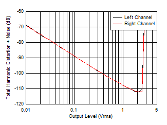
INA1620 THDN_vs_level_32_ohm.gif
22.4-kHz measurement bandwidth
Figure 57. THD+N vs Output Voltage for a 32-Ω Load
INA1620 FFT_Left_Channel_32_ohm.gif
1 kHz, 32-Ω load, 1 VRMS
Figure 59. Output Spectrum
INA1620 THDN_vs_Frequency_32_ohm.gif
90-kHz measurement bandwidth, 1-VRMS output
Figure 58. THD+N vs Frequency for a 32-Ω Load