ZHCSIG1D August 2016 – September 2023 DS90UB960-Q1
PRODUCTION DATA
- 1
- 1 特性
- 2 应用
- 3 说明
- 4 Revision History
- 5 Pin Configuration and Functions
-
6 Specifications
- 6.1 Absolute Maximum Ratings
- 6.2 ESD Ratings
- 6.3 Recommended Operating Conditions
- 6.4 Thermal Information
- 6.5 DC Electrical Characteristics
- 6.6 AC Electrical Characteristics
- 6.7 CSI-2 Timing Specifications
- 6.8 Recommended Timing for the Serial Control Bus
- 6.9 Timing Diagrams
- 6.10 Typical Characteristics
-
7 Detailed Description
- 7.1 Overview
- 7.2 Functional Block Diagram
- 7.3 Feature Description
- 7.4
Device Functional Modes
- 7.4.1 CSI-2 Mode
- 7.4.2 RAW Mode
- 7.4.3 MODE Pin
- 7.4.4 REFCLK
- 7.4.5 Receiver Port Control
- 7.4.6 Input Jitter Tolerance
- 7.4.7 Adaptive Equalizer
- 7.4.8 Channel Monitor Loop-Through Output Driver
- 7.4.9 RX Port Status
- 7.4.10 Sensor Status
- 7.4.11 GPIO Support
- 7.4.12 RAW Mode LV / FV Controls
- 7.4.13 CSI-2 Protocol Layer
- 7.4.14 CSI-2 Short Packet
- 7.4.15 CSI-2 Long Packet
- 7.4.16 CSI-2 Data Identifier
- 7.4.17 Virtual Channel and Context
- 7.4.18 CSI-2 Mode Virtual Channel Mapping
- 7.4.19 CSI-2 Transmitter Frequency
- 7.4.20 CSI-2 Output Bandwidth
- 7.4.21 CSI-2 Transmitter Status
- 7.4.22 Video Buffers
- 7.4.23 CSI-2 Line Count and Line Length
- 7.4.24 FrameSync Operation
- 7.4.25
CSI-2 Forwarding
- 7.4.25.1 Best-Effort Round Robin CSI-2 Forwarding
- 7.4.25.2 Synchronized CSI-2 Forwarding
- 7.4.25.3 Basic Synchronized CSI-2 Forwarding
- 7.4.25.4 Line-Interleaved CSI-2 Forwarding
- 7.4.25.5 Line-Concatenated CSI-2 Forwarding
- 7.4.25.6 CSI-2 Replicate Mode
- 7.4.25.7 CSI-2 Transmitter Output Control
- 7.4.25.8 Enabling and Disabling CSI-2 Transmitters
- 7.5
Programming
- 7.5.1 Serial Control Bus
- 7.5.2 Second I2C Port
- 7.5.3 I2C Target Operation
- 7.5.4 Remote Target Operation
- 7.5.5 Remote Target Addressing
- 7.5.6 Broadcast Write to Remote Devices
- 7.5.7 I2C Controller Proxy
- 7.5.8 I2C Controller Proxy Timing
- 7.5.9 Interrupt Support
- 7.5.10 Error Handling
- 7.5.11 Timestamp – Video Skew Detection
- 7.5.12 Pattern Generation
- 7.5.13 FPD-Link BIST Mode
- 7.6 Register Maps
- 8 Application and Implementation
- 9 Device and Documentation Support
- 10Mechanical, Packaging, and Orderable Information
8.5.2 Layout Example
Stencil parameters such as aperture area ratio and the fabrication process have a significant impact on paste deposition. Inspection of the stencil prior to placement of the VQFN package is highly recommended to improve board assembly yields. If the via and aperture openings are not carefully monitored, the solder may flow unevenly through the DAP.
Example PCB layout is used to demonstrate both proper routing and proper solder techniques when designing in the Deserializer.
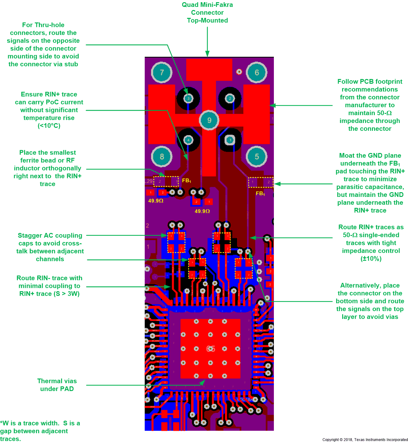
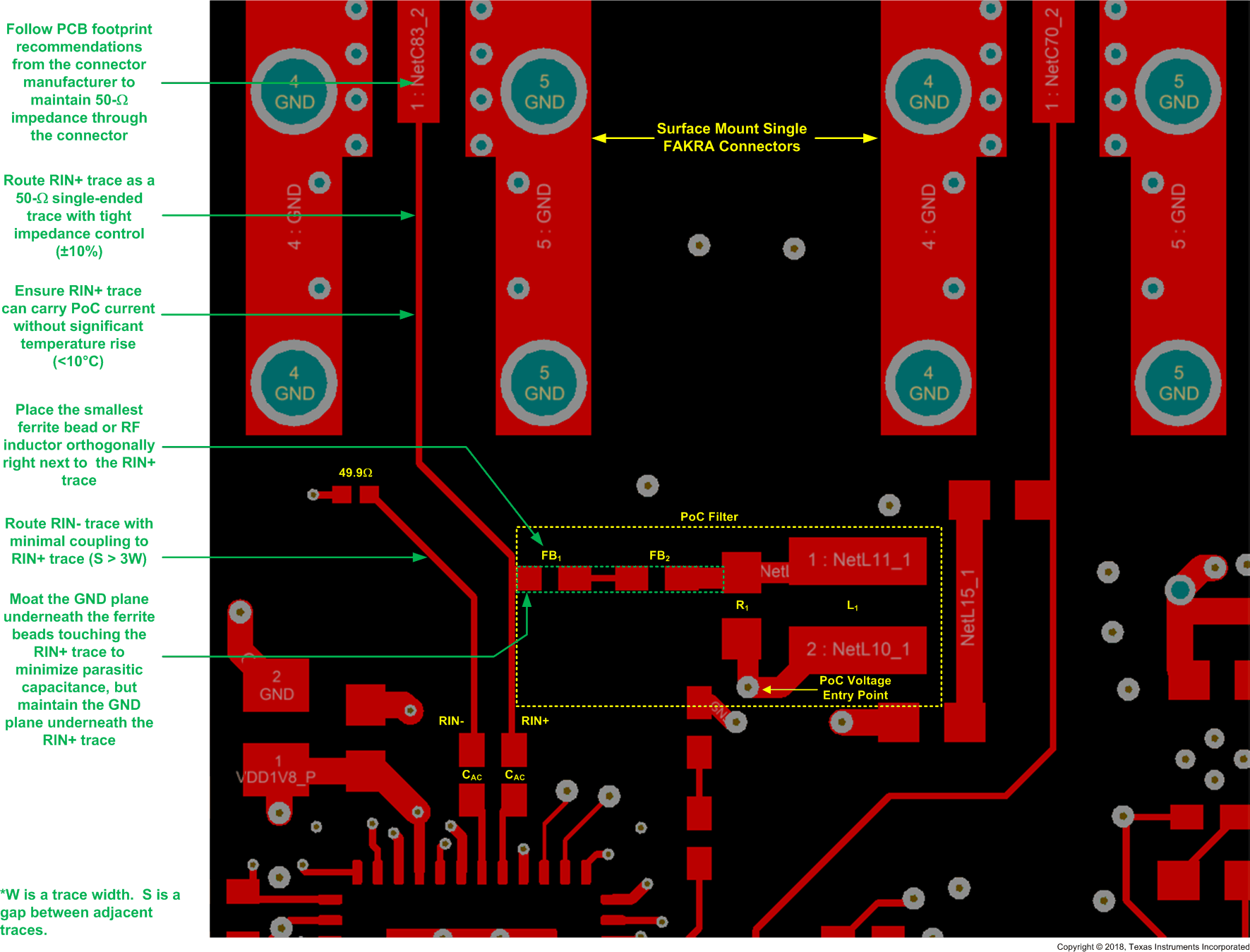
Figure 8-21 shows a PCB layout example are derived from the layout design of the DS90UB960-Q1EVM Evaluation Board. The graphic and layout description are used to determine proper routing when designing the board. The high-speed FPD-Link III traces routed differentially up to the connector. A 100-Ω differential characteristic impedance and 50-Ω single-ended characteristic impedance traces are maintained as much as possible for both STP and coaxial applications. For the layout of a coaxial interconnects, coupled traces should be used with the RINx- termination near to the connector.
 Figure 8-21 DS90UB960-Q1 Example PCB Layout With Quad Mini-Fakra Connector
 Figure 8-22 Example Routing of FPD-Link III Traces to a Single Mini-Fakra Connector and PoC Components
 Figure 8-23 Example Routing of CSI-2 Traces