ZHCSFV6E august 2016 – november 2020 DS90UB933-Q1
PRODUCTION DATA
- 1
- 1 特性
- 2 应用
- 3 说明
- 4 Revision History
- 5 Pin Configuration and Functions
-
6 Specifications
- 6.1 Absolute Maximum Ratings
- 6.2 ESD Ratings
- 6.3 Recommended Operating Conditions
- 6.4 Thermal Information
- 6.5 Electrical Characteristics
- 6.6 Recommended Serializer Timing For PCLK
- 6.7 AC Timing Specifications (SCL, SDA) - I2C-Compatible
- 6.8 Bidirectional Control Bus DC Timing Specifications (SCL, SDA) - I2C-Compatible
- 6.9 Serializer Switching Characteristics
- 6.10 Timing Diagrams
- 6.11 Typical Characteristics
- 7 Detailed Description
- 8 Application and Implementation
- 9 Power Supply Recommendations
- 10Layout
- 11Device and Documentation Support
7.5.6 Multiple Device Addressing
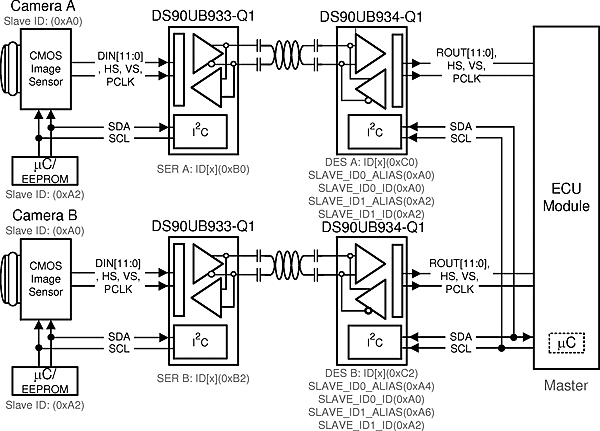
Some applications require multiple camera devices with the same fixed address to be accessed on the same I2C bus. The DS90UB933-Q1 provides slave ID matching/aliasing to generate different target slave addresses when connecting more than two identical devices together on the same bus. This allows the slave devices to be independently addressed. Each device connected to the bus is addressable through a unique ID by programming of the slave alias register on deserializer. This remaps the slave alias address to the target SLAVE_ID address; up to 8 ID aliases are supported in sensor mode when slaves are attached to the DS90UB933-Q1 serializer. In display mode, when the external slaves are at the deserializer the DS90UB933-Q1 supports one ID alias. The ECU controller must keep track of the list of I2C peripherals in order to properly address the target device.
See Figure 7-15 for an example of this function.
- ECU is the I2C master and has an I2C master interface.
- The I2C interfaces in DES A and DES B are both slave interfaces.
- The I2C protocol is bridged from DES A to SER A and from DES B to SER B.
- The I2C interfaces in SER A and SER B are both master interfaces.
If master controller transmits I2C slave 0xA0, DES A (address 0xC0), with pass-through enabled, forwards the transaction to remote Camera A. If the controller transmits slave address 0xA4, the DES B 0xC2 recognizes that 0xA4 is mapped to 0xA0 and is transmitted to the remote Camera B. If controller sends command to address 0xA6, the DES B (address 0xC2), with pass-through enabled, forwards the transaction to slave device 0xA2.
 Figure 7-15 Multiple Device Addressing