ZHCSDY9A June 2015 – July 2015 DRV8881
PRODUCTION DATA.
- 1 特性
- 2 应用
- 3 说明
- 4 修订历史记录
- 5 Pin Configuration and Functions
- 6 Specifications
-
7 Detailed Description
- 7.1 Overview
- 7.2 Functional Block Diagrams
- 7.3
Feature Description
- 7.3.1 Motor Driver Current Ratings
- 7.3.2 PWM Motor Drivers
- 7.3.3 Bridge Control
- 7.3.4 Current Regulation
- 7.3.5 Decay Modes
- 7.3.6 AutoTune
- 7.3.7 Adaptive Blanking Time
- 7.3.8 Parallel Mode
- 7.3.9 Charge Pump
- 7.3.10 LDO Voltage Regulator
- 7.3.11 Logic and Tri-Level Pin Diagrams
- 7.3.12 Protection Circuits
- 7.4 Device Functional Modes
- 8 Application and Implementation
- 9 Power Supply Recommendations
- 10Layout
- 11器件和文档支持
- 12机械、封装和可订购信息
封装选项
机械数据 (封装 | 引脚)
散热焊盘机械数据 (封装 | 引脚)
订购信息
8 Application and Implementation
NOTE
Information in the following applications sections is not part of the TI component specification, and TI does not warrant its accuracy or completeness. TI’s customers are responsible for determining suitability of components for their purposes. Customers should validate and test their design implementation to confirm system functionality.
8.1 Application Information
The DRV8881 is used in stepper or brushed motor control.
8.2 Typical Applications
8.2.1 DRV8881P Typical Application
The following design procedure can be used to configure the DRV8881. In this application, the DRV8881P will be used to drive a stepper motor.
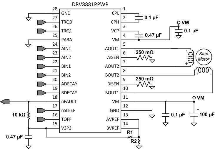 Figure 24. Typical Application Schematic
8.2.1.1 Design Requirements
Table 9 gives design input parameters for system design.
Table 9. Design Parameters
| DESIGN PARAMETER | REFERENCE | EXAMPLE VALUE |
|---|---|---|
| Supply voltage | VM | 24 V |
| Motor winding resistance | RL | 4.5 Ω/phase |
| Motor winding inductance | LL | 10.5 mH/phase |
| Motor full step angle | θstep | 1.8°/step |
| Target microstepping level | nm | Non-circular 1/2 step |
| Target motor speed | v | 120 rpm |
| Target full-scale current | IFS | 800 mA |
8.2.1.2 Detailed Design Procedure
8.2.1.2.1 Current Regulation
In a stepper motor, the full-scale current (IFS) is the maximum current driven through either winding. This quantity will depend on the TRQ pins, the xVREF analog voltage, and the sense resistor value (RSENSE). AVREF and BVREF can be configured to drive different currents, but in this example the same full-scale current is used in both coils.

TRQ is a DAC used to scale the output current. The current scalar value for different inputs is shown in Table 10.
Table 10. Torque DAC Settings
| TRQ1 | TRQ0 | CURRENT SCALAR (TRQ) |
|---|---|---|
| 1 | 1 | 25% |
| 1 | 0 | 50% |
| 0 | 1 | 75% |
| 0 | 0 | 100% |
| Example: If the desired full-scale current is 800 mA | ||
| Set RSENSE = 250 mΩ, assume TRQ = 100%. | ||
| xVREF would have to be 1.32 V. | ||
| Create a resistor divider from V3P3 (3.3 V) to set AVREF and BVREF ≈ 1.32 V. | ||
| Set R2 = 10 kΩ, set R1 = 15 kΩ | ||
Note that IFS must also follow Equation 3 in order to avoid saturating the motor. VM is the motor supply voltage, and RL is the motor winding resistance.

8.2.1.2.2 Stepper Motor Speed
Next, the driving waveform needs to be planned. In order to command the correct speed, determine the frequency of the input waveform.
If the target motor speed is too high, the motor will not spin. Make sure that the motor can support the target speed.
For a desired motor speed (v), microstepping level (nm), and motor full step angle (θstep),

θstep can be found in the stepper motor data sheet or written on the motor itself.
The frequency ƒstep gives the frequency of input change on the DRV8881P. 1/ ƒstep = tSTEP on the diagram below.

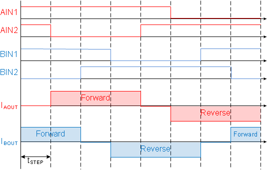 Figure 25. Example 1/2 Stepping Operation
8.2.1.2.3 Decay Modes
The DRV8881 supports several different decay modes: slow decay, fast decay, mixed decay, and AutoTune (DRV8881E only). The current through the motor windings is regulated using an adjustable fixed-time-off scheme. This means that after any drive phase, when a motor winding current has hit the current chopping threshold (ITRIP), the DRV8881 will place the winding in one of the decay modes for TOFF. After TOFF, a new drive phase starts.
8.2.1.2.4 Sense Resistor
For optimal performance, it is important for the sense resistor to be:
- Surface-mount
- Low inductance
- Rated for high enough power
- Placed closely to the motor driver
The power dissipated by the sense resistor equals Irms2 × R. For example, if the rms motor current is 1.4 A and a 250 mΩ sense resistor is used, the resistor will dissipate 1.4 A2 × 0.25 Ω = 0.49 W. The power quickly increases with higher current levels.
Resistors typically have a rated power within some ambient temperature range, along with a derated power curve for high ambient temperatures. When a PCB is shared with other components generating heat, margin should be added. It is always best to measure the actual sense resistor temperature in a final system, along with the power MOSFETs, as those are often the hottest components.
Because power resistors are larger and more expensive than standard resistors, it is common practice to use multiple standard resistors in parallel, between the sense node and ground. This distributes the current and heat dissipation.
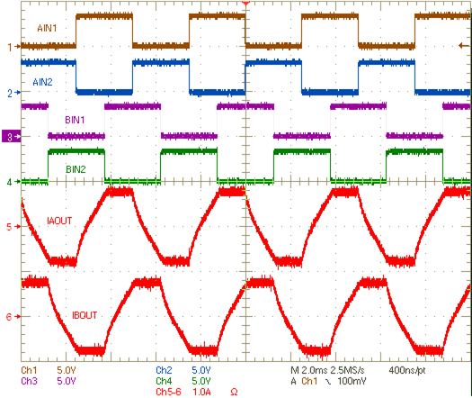
8.2.1.3 Application Curve
8.2.2 Alternate Application
In this application, the DRV8881P will be operated in parallel mode in order to drive a single brushed-DC motor.
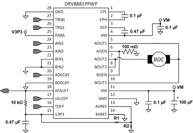 Figure 27. Typical Application Schematic
8.2.2.1 Design Requirements
Table 11 gives design input parameters for system design.
Table 11. Design Parameters
| DESIGN PARAMETER | REFERENCE | EXAMPLE VALUE |
|---|---|---|
| Supply voltage | VM | 24 V |
| Motor winding resistance | RL | 6 Ω |
| Motor winding inductance | LL | 4.1 mH |
| Target maximum motor current | ITRIP | 2 A |
8.2.2.2 Detailed Design Procedure
8.2.2.2.1 Current Regulation
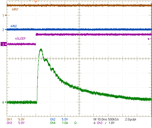
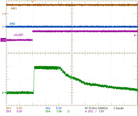
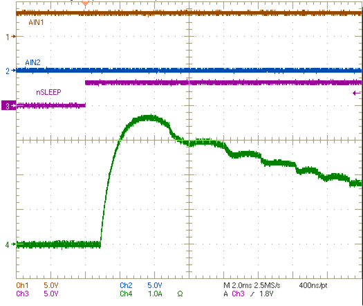
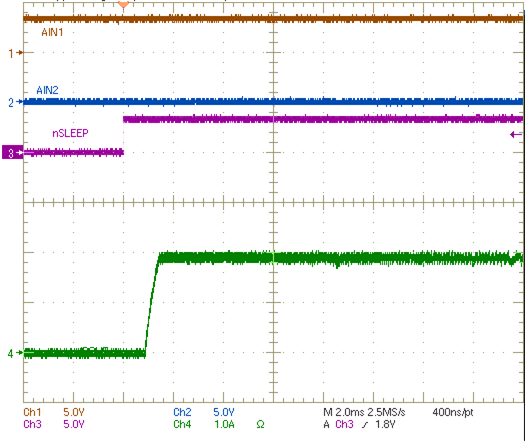
The maximum current (ITRIP) is set by the TRQ pins, the xVREF analog voltage, and the sense resistor value (RSENSE). In parallel mode the winding current is set by AVREF only and BVREF is ignored. When starting a brushed-DC motor, a large inrush current may occur because there is no back-EMF. Current regulation will act to limit this inrush current and prevent high current on startup.
| Example: If the desired regulation current is 2 A | ||
| Set RSENSE = 100 mΩ, assume TRQ = 100%. | ||
| AVREF would have to be 1.32 V. | ||
| Create a resistor divider from V3P3 (3.3 V) to set AVREF ≈ 1.32 V: Set R2 = 10 kΩ, set R1 = 15 kΩ | ||
8.2.2.3 Application Curves
