ZHCSC08C December 2013 – August 2015 DLPC6401
PRODUCTION DATA.
- 1 特性
- 2 应用
- 3 说明
- 4 修订历史记录
- 5 Pin Configuration and Functions
-
6 Specifications
- 6.1 Absolute Maximum Ratings
- 6.2 ESD Ratings
- 6.3 Recommended Operating Conditions
- 6.4 Thermal Information
- 6.5 Electrical Characteristics
- 6.6 Electrical Characteristics (Normal Mode)
- 6.7 System Oscillators Timing Requirements
- 6.8 Test and Reset Timing Requirements
- 6.9 JTAG Interface: I/O Boundary Scan Application Timing Requirements
- 6.10 Port 1 Input Pixel Interface Timing Requirements
- 6.11 Port 2 Input Pixel Interface (FPD-Link Compatible LVDS Input) Timing Requirements
- 6.12 Synchronous Serial Port (SSP) Interface Timing Requirements
- 6.13 Programmable Output Clocks Switching Characteristics
- 6.14 Synchronous Serial Port (SSP) Interface Switching Characteristics
- 6.15 JTAG Interface: I/O Boundary Scan Application Switching Characteristics
- 7 Detailed Description
- 8 Application and Implementation
- 9 Power Supply Recommendations
- 10Layout
- 11器件和文档支持
- 12机械、封装和可订购信息
6 Specifications
6.1 Absolute Maximum Ratings
over recommended operating free-air temperature (unless otherwise noted) (1)| MIN | MAX | UNIT | |||
|---|---|---|---|---|---|
| ELECTRICAL | |||||
| Supply voltage(2) | VDDC (core 1.2-V power) | –0.5 | 1.7 | V | |
| VDD33 (CMOS I/O) | –0.5 | 3.8 | |||
| VDD_DMD (DMD driver power) | –0.5 | 2.3 | |||
| VDD12_FPD (FPD-Link LVDS interface 1.2-V power) | –0.5 | 1.7 | |||
| VDD33_FPD (FPD-Link LVDS interface 3.3-V power) | –0.5 | 3.8 | |||
| VDD12_PLLD (DDR clock generator – digital) | –0.5 | 1.7 | |||
| VDD12_PLLM (master clock generator – digital) | –0.5 | 1.7 | |||
| VDD_18_PLLD (DDR clock generator – analog) | –0.5 | 2.3 | |||
| VDD_18_PLLM (master clock generator – analog) | –0.5 | 2.3 | |||
| VI | Input voltage(3) | OSC (BC1850) | –0.3 | 3.6 | |
| LVCMOS (BT3350) | –0.5 | 3.6 | |||
| I2C (BT3350) | –0.5 | 3.6 | |||
| LVDS (BT3350) | –0.5 | 3.6 | |||
| VO | Output voltage | DMD LPDDR (BC1850) | –0.3 | 2.0 | |
| LVCMOS (BT3350) | –0.5 | 3.6 | |||
| I2C (BT3350) | –0.5 | 3.6 | |||
| ENVIRONMENTAL | |||||
| TJ | Operating junction temperature | 0 | 115 | °C | |
| Tstg | Storage temperature | –40 | 125 | °C | |
(1) Stresses beyond those listed under Absolute Maximum Ratings may cause permanent damage to the device. These are stress ratings only, which do not imply functional operation of the device at these or any other conditions beyond those indicated under Recommended Operating Conditions. Exposure to absolute-maximum-rated conditions for extended periods may affect device reliability.
(2) All voltage values are with respect to GND.
(3) Applies to external input and bidirectional buffers.
6.2 ESD Ratings
| VALUE | UNIT | |||
|---|---|---|---|---|
| V(ESD) | Electrostatic discharge | Human body model (HBM), per ANSI/ESDA/JEDEC JS-001, all pins(1) | ±2000 | V |
| Charged device model (CDM), per JEDEC specification JESD22-C101, all pins(2) | ±500 | |||
| Machine model (MM) | ±150 | |||
(1) JEDEC document JEP155 states that 500-V HBM allows safe manufacturing with a standard ESD control process.
(2) JEDEC document JEP157 states that 250-V CDM allows safe manufacturing with a standard ESD control process.
6.3 Recommended Operating Conditions
over operating free-air temperature range (unless otherwise noted)| I/O(1) | MIN | NOM | MAX | UNIT | ||
|---|---|---|---|---|---|---|
| VDD33 | 3.3-V supply voltage, I/O | 3.135 | 3.3 | 3.465 | V | |
| VDD_DMD | 1.9-V supply voltage, I/O | 1.8 | 1.9 | 2 | V | |
| VDD_18_PLLD | 1.8-V supply voltage, PLL analog | 1.71 | 1.8 | 1.89 | V | |
| VDD_18_PLLM | 1.8-V supply voltage, PLL analog | 1.71 | 1.8 | 1.89 | V | |
| VDD12 | 1.2-V supply voltage, core logic | 1.116 | 1.2 | 1.26 | V | |
| VDD12_PLLD | 1.2-V supply voltage, PLL digital | 1.116 | 1.2 | 1.26 | V | |
| VDD12_PLLM | 1.2-V supply voltage, PLL digital | 1.116 | 1.2 | 1.26 | V | |
| VI | Input voltage | OSC (10) | 0 | VDD33 | V | |
| 3.3-V LVCMOS (1, 2, 3, 4) | 0 | VDD33 | ||||
| 3.3-V I2C (8) | 0 | VDD33 | ||||
| 3.3-V LVDS (5) | 0.6 | 2.2 | ||||
| VO | Output voltage | 3.3-V LVCMOS (1, 2, 3, 4) | 0 | VDD33 | V | |
| 3.3-V I2C (8) | 0 | VDD33 | ||||
| 1.9-V LPDDR (7) | 0 | VDD_DMD | ||||
| TA | Operating ambient temperature range | See (2) | 0 | 55 | °C | |
| TC | Operating top-center case temperature | See (3)(4) | 0 | 104 | °C | |
| TJ | Operating junction temperature | 0 | 105 | °C | ||
(1) The number inside each parenthesis for the I/O refers to the type defined in the I/O type subscript definition section.
(2) Assumes a minimum 1-m/s airflow along with the JEDEC thermal resistance and associated conditions as listed www.ti.com/packaging. Thus, this is an approximate value that varies with environment and PCB design.
(3) Maximum thermal values assume maximum power of 3 W.
(4) Assume ψJT equals 0.33 C/W.
6.4 Thermal Information(1)
| THERMAL METRIC(1) | DLPC6401 | UNIT | |
|---|---|---|---|
| ZFF (BGA) | |||
| 419 PINS | |||
| ψJT | Junction-to-top characterization parameter | 0.33 | °C/W |
(1) For more information about traditional and new thermal metrics, see the Semiconductor and IC Package Thermal Metrics Application Report, SPRA953.
6.5 Electrical Characteristics(1)
over operating free-air temperature range (unless otherwise noted)(1) The number inside each parenthesis for the I/O refers to the type defined in Table 1.
6.6 Electrical Characteristics (Normal Mode)
over operating free-air temperature range (unless otherwise noted)| PARAMETER | TEST CONDITION(2) | MIN | TYP | MAX(1) | UNIT | |
|---|---|---|---|---|---|---|
| ICC12 | Supply voltage, 1.2-V core power | Normal mode | 600 | 1020 | mA | |
| ICC19_DMD | Supply voltage, 1.9-V I/O power (DMD LPDDR) | Normal mode | 30 | 50 | mA | |
| ICC33 | Supply voltage, 3.3-V (I/O) power | Normal mode | 40 | 70 | mA | |
| ICC12_FPD | FPD-Link LVDS I/F supply voltage, 1.2-V power | Normal mode | 60 | 100 | mA | |
| ICC33_FPD | FPD-Link LVDS I/F supply voltage, 3.3-V power | Normal mode | 50 | 85 | mA | |
| ICC12_PLLD | Supply voltage, PLL digital power (1.2 V) | Normal mode | 9 | 15 | mA | |
| ICC12_PLLM | Supply voltage, master clock generator PLL digital power (1.2 V) | Normal mode | 9 | 15 | mA | |
| ICC18_PLLD | Supply voltage, PLL analog power (1.8 V) | Normal mode | 10 | 16 | mA | |
| ICC18_PLLM | Supply voltage, master clock generator PLL analog power (1.8 V) | Normal mode | 10 | 16 | mA | |
| PTOT | Total power | Normal mode | 1225 | 2200 | mW | |
(1) Maximum power values are estimates and may not reflect the actual final power consumption of DLPC6401 ASIC.
(2) Normal mode refers to ASIC operation during full functionality, active product operation. Typical values correspond to power dissipated on nominal process devices operating at nominal voltage and 70°C junction temperature (approximately 25°C ambient) displaying typical video-graphics content from a high-frequency source. Maximim values correspond to power dissipated on fast process devices operating at high voltage and 105°C junction temperature (approximately 55°C ambient) displaying typical video-graphics content from a high-frequency source. The increased power dissipation observed on fast process devices operated at maximum recommended temperature is primarily a result of increased leakage current.
6.7 System Oscillators Timing Requirements
over operating free-air temperature range (unless otherwise noted)| MIN | MAX | UNIT | |||
|---|---|---|---|---|---|
| ƒclock | Clock frequency, MOSC(1) | 31.9968 | 32.0032 | MHz | |
| tc | Cycle time, MOSC(1) | 31.188 | 31.256 | ns | |
| tw(H) | Pulse duration(2), MOSC, high | 50% to 50% reference points (signal) | 12.5 | ns | |
| tw(L) | Pulse duration(2), MOSC, low | 50% to 50% reference points (signal) | 12.5 | ns | |
| tt | Transition time(2), MOSC, tt = tf / tr | 20% to 80% reference points (signal) | 7.5 | ns | |
| tjp | Period jitter(2), MOSC (that is, the deviation in period from ideal period due solely to high-frequency jitter – not spread spectrum clocking) | –100 | 100 | ps | |
(1) The frequency range for MOSC is 32 MHz with ±100 PPM accuracy. (This includes impact to accuracy due to aging, temperature, and trim sensitivity.) The MOSC input cannot support spread spectrum clock spreading.
(2) Applies only when driven by an external digital oscillator.
6.8 Test and Reset Timing Requirements
| MIN | MAX | UNIT | |||
|---|---|---|---|---|---|
| tW1(L) | Pulse duration, inactive low, PWRGOOD | 50% to 50% reference points (signal) | 4 | µs | |
| tt1 | Transition time, PWRGOOD, tt1 = tf / tr | 20% to 80% reference points (signal) | 625 | µs | |
| tW2(L) | Pulse duration, inactive low, POSENSE | 50% to 50% reference points (signal) | 500 | µs | |
| tt2 | Transition time, POSENSE, tt2 = tf / tr | 20% to 80% reference points (signal) | 1 | µs | |
| tPH | Power hold time, POSENSE remains active after PWGOOD is deasserted | 20% to 80% reference points (signal) | 500 | µs | |
6.9 JTAG Interface: I/O Boundary Scan Application Timing Requirements
| MIN | MAX | UNIT | |||
|---|---|---|---|---|---|
| ƒclock | Clock frequency, TCK | 10 | MHz | ||
| tC | Cycle time, TCK | 100 | ns | ||
| tW(H) | Pulse duration, high | 50% to 50% reference points (signal) | 40 | ns | |
| tW(L) | Pulse duration, low | 50% to 50% reference points (signal) | 40 | ns | |
| tt | Transition time, tt = tf / tr | 20% to 80% reference points (signal) | 5 | ns | |
| tSU | Setup time, TDI valid before TCK↑ | 8 | ns | ||
| th | Hold time, TDI valid after TCK↑ | 2 | ns | ||
| tSU | Setup time, TMS1 valid before TCK↑ | 8 | ns | ||
| th | Hold time, TMS1 valid after TCK↑ | 2 | ns | ||
6.10 Port 1 Input Pixel Interface Timing Requirements
| MIN | MAX | UNIT | |||
|---|---|---|---|---|---|
| ƒclock | Clock frequency, P1A_CLK, P1B_CLK, P1C_CLK | 12 | 150 | MHz | |
| tc | Cycle time, P1A_CLK, P1B_CLK, P1C_CLK | 6.666 | 83.33 | ns | |
| tw(H) | Pulse duration, high | 50% to 50% reference points (signal) | 2.3 | ns | |
| tw(L) | Pulse duration, low | 50% to 50% reference points (signal) | 2.3 | ns | |
| tjp | Clock period jitter, P1A_CLK, P1B_CLK, P1C_CLK (that is, the deviation in period from ideal period) |
Max ƒclock | See (2) | ps | |
| tt | Transition time, tt = tf / tr, P1A_CLK, P1B_CLK, P1C_CLK | 20% to 80% reference points (signal) | 0.6 | 2 | ns |
| tt | Transition time, tt = tf / tr, P1_A(9-0), P1_B(9-0) , P1_C(9-0), P1_HSYNC, P1_VSYNC, P1_DATEN | 20% to 80% reference points (signal) | 0.6 | 3 | ns |
| tt | Transition time, tt = tf / tr, ALF_HSYNC, ALF_VSYNC, ALF_CSYNC(1) | 20% to 80% reference points (signal) | 0.6 | 3 | ns |
| SETUP AND HOLD TIMES(3) | |||||
| tsu | Setup time, P1_A(9-0), valid before P1x_CLK↑↓ | 0.8 | ns | ||
| th | Hold time, P1_A(9-0), valid after P1x_CLK↑↓ | 0.8 | ns | ||
| tsu | Setup time, P1_B(9-0), valid before P1x_CLK↑↓ | 0.8 | ns | ||
| th | Hold time, P1_B(9-0), valid after P1x_CLK↑↓ | 0.8 | ns | ||
| tsu | Setup time, P1_C(9-0), valid before P1x_CLK↑↓ | 0.8 | ns | ||
| th | Hold time, P1_C(9-0), valid after P1x_CLK↑↓ | 0.8 | ns | ||
| tsu | Setup time, P1_VSYNC, valid before P1x_CLK↑↓ | 0.8 | ns | ||
| th | Hold time, P1_VSYNC, valid after P1x_CLK↑↓ | 0.8 | ns | ||
| tsu | Setup time, P1_HSYNC, valid before P1x_CLK↑↓ | 0.8 | ns | ||
| th | Hold time, P1_HSYNC, valid after P1x_CLK↑↓ | 0.8 | ns | ||
| tsu | Setup time, P1_FIELD, valid before P1x_CLK↑↓ | 0.8 | ns | ||
| th | Hold time, P1_FIELD, valid after P1x_CLK↑↓ | 0.8 | ns | ||
| tsu | Setup time, P1_DATEN, valid before P1x_CLK↑↓ | 0.8 | ns | ||
| th | Hold time, P1_DATEN, valid after P1x_CLK↑↓ | 0.8 | ns | ||
(1) ALF_CSYNC, ALF_VSYNC and ALF_HSYNC are asynchronous signals.
(2) Use the following formula to obtain the jitter: Maximum clock jitter = ±[(1 / ƒclock) – 5414 ps].
(3) Setup and hold times should be considered the same regardless of clock used [P1A_CLK, P1B_CLK, P1C_CLK].
6.11 Port 2 Input Pixel Interface (FPD-Link Compatible LVDS Input) Timing Requirements(1)(2)(3)(4)(5)(6)
| MIN | MAX | UNIT | ||
|---|---|---|---|---|
| ƒclock | Clock frequency, P2_CLK (LVDS input clock) | 20 | 90 | MHz |
| tc | Cycle time, P2_CLK (LVDS input clock) | 11.1 | 50 | ns |
| tslew | Clock or data slew rate (ƒpxck < 90 MHz) | 0.3 | V/ns | |
| Clock or data slew rate (ƒpxck > 90 MHz) | 0.5 | V/ns | ||
| tstartup | Link start-up time (internal) | 1 | ms | |
(1) Minimize crosstalk and match traces on the PCB as close as possible.
(2) Maintain the common mode voltage as close to 1.2 V as possible.
(3) Maintain the absolute input differential voltage as high as possible.
(4) The LVDS open input detection is related to a low common mode voltage only. It is not related to a low-differential swing.
(5) LVDS power 3.3-V supply (VDD33_FPD) noise level should be below 100 mVPP.
(6) LVDS power 1.2-V supply (VDD12_FPD) noise level should be below 60 mVPP.
6.12 Synchronous Serial Port (SSP) Interface Timing Requirements
| MIN | MAX | UNIT | ||
|---|---|---|---|---|
| tsu | Setup time, SSP0_RXD valid before SSP0_ CLK↓ | 10 | ns | |
| th | Hold time, SSP0_RXD valid after SSP0_ CLK↓ | 10 | ns | |
| tt | Transition time(1), SSP0_RXD, tt = tf / tr | 4 | ns | |
| tsu | Setup time, SSP1_RXD valid before SSP1_ CLK↓ | 10 | ns | |
| th | Hold time, SSP1_RXD valid after SSP1_ CLK↓ | 10 | ns | |
| tt | Transition time(1), SSP1_RXD, tt = tf / tr | 4 | ns | |
(1) 20% to 80% reference points (signal)
6.13 Programmable Output Clocks Switching Characteristics
over operating free-air temperature range, CL (min timing) = 5 pF, CL (max timing) = 50 pF (unless otherwise noted) (see Figure 5)| PARAMETER | FROM (INPUT) | TO (OUTPUT) | MIN | MAX | UNIT | |
|---|---|---|---|---|---|---|
| ƒclock | Clock frequency, OCLKC(1) | N/A | OCLKC | 0.7759 | 48 | MHz |
| tc | Cycle time, OCLKC(1) | N/A | OCLKC | 20.83 | 1288.8 | ns |
| tw(H) | Pulse duration, high 50% to 50% reference points (signal) | N/A | OCLKC | (tc / 2) – 2 | ns | |
| tw(L) | Pulse duration, low(2) 50% to 50% reference points (signal) | N/A | OCLKC | (tc / 2) – 2 | ns | |
| ƒclock | Clock frequency, OCLKD(1) | N/A | OCLKD | 0.7759 | 48 | MHz |
| tc | Cycle time, OCLKD | N/A | OCLKD | 20.83 | 1288.8 | ns |
| tw(H) | Pulse duration, high(2) 50% to 50% reference points (signal) | N/A | OCLKD | (tc / 2) – 2 | ns | |
| tw(L) | Pulse duration, low(2) 50% to 50% reference points (signal) | N/A | OCLKD | (tc / 2) – 2 | ns | |
| ƒclock | Clock frequency, OCLKE(1) | N/A | OCLKE | 0.7759 | 48 | MHz |
| tc | Cycle time, OCLKE | N/A | OCLKE | 20.83 | 1288.8 | ns |
| tw(H) | Pulse duration, high(2) 50% to 50% reference points (signal) | N/A | OCLKE | (tc / 2) – 2 | ns | |
| tw(L) | Pulse duration, low(2) 50% to 50% reference points (signal) | N/A | OCLKE | (tc / 2) – 2 | ns | |
(1) The frequency of OCLKC through OCLKE is programmable.
(2) The duty cycle of OCLKC through OCLKE is within ±2 ns of 50%.
6.14 Synchronous Serial Port (SSP) Interface Switching Characteristics
over recommended operating conditions, CL (min timing) = 5 pF, CL (max timing) = 35 pF (unless otherwise noted) (see Figure 10)| PARAMETER | FROM (INPUT) | TO (OUTPUT) | MIN | MAX | UNIT | |
|---|---|---|---|---|---|---|
| ƒclock | Clock frequency, SSP0_CLK (1)(2) | N/A | SSP0_CLK | 0.287 | 9333 | kHz |
| tc | Cycle time, SSP0_CLK | N/A | SSP0_CLK | 0.107 | 3483 | us |
| tw(H) | Pulse duration, high 50% to 50% reference points (signal) | N/A | SSP0_CLK | 48 | ns | |
| tw(L) | Pulse duration, low 50% to 50% reference points (signal) | N/A | SSP0_CLK | 48 | ns | |
| tpd | Output propagation, clock to Q, SSP0_TXD | SSP0_CLK↑ | SSP0_TXD | –5 | 5 | ns |
| ƒclock | Clock frequency, SSP1_CLK (1)(2) | N/A | SSP1_CLK | 2.296 | 74667 | kHz |
| tc | Cycle time, SSP1_CLK | N/A | SSP1_CLK | 0.013 | 436 | us |
| tw(H) | Pulse duration, high 50% to 50% reference points (signal) | N/A | SSP1_CLK | 5.85 | ns | |
| tw(L) | Pulse duration, low 50% to 50% reference points (signal) | N/A | SSP1_CLK | 5.85 | ns | |
| tpd | Output propagation, clock to Q, SSP1_TXD | SSP1_CLK↑ | SSP1_TXD | –2 | 2 | ns |
(1) SSP output timing supports both positive and negative clocking polarity. Figure 10 shows only positive clocking polarity. When the clock polarity is configured through software to be negative, the data is transferred and captured on the opposite edge of the clock shown.
(2) The maximum rates shown apply to master mode operation only. Slave mode operation is limited to 1/6 of these rates.
6.15 JTAG Interface: I/O Boundary Scan Application Switching Characteristics
Over operating free-air temperature range, CL (min timing) = 5 pF, CL (max timing) = 85 pF (unless otherwise noted)| PARAMETER | FROM (INPUT) | TO (OUTPUT) | MIN | TYP | MAX | UNIT | |
|---|---|---|---|---|---|---|---|
| tpd | Output propagation, clock to Q | TCK↓ | TDO1 | 3 | 12 | ns | |
 Figure 1. System Oscillators
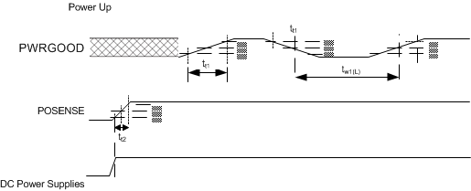
PWRGOOD has no impact on operation for 60 ms after rising edge of POSENSE.
Figure 2. Power Up
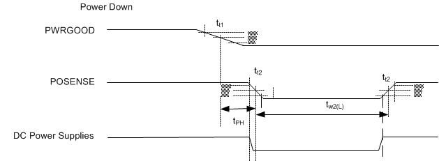 Figure 3. Power Down
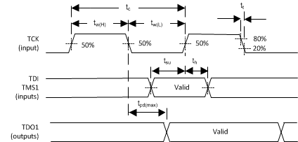 Figure 4. I/O Boundary Scan
 Figure 5. Programmable Output Clocks
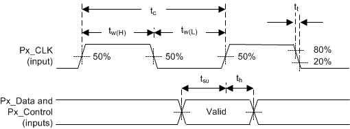 Figure 6. Input Port 1 Interface
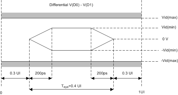 Figure 7. Input Port 2 (LVDS) Interface
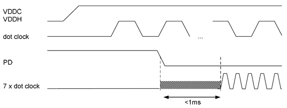 Figure 8. (LVDS) Link Start-Up Timing
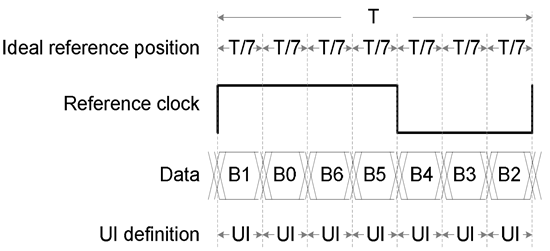 Figure 9. (LVDS) Clock – Data Skew Definition
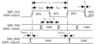 Figure 10. Synchronous Serial Port Interface
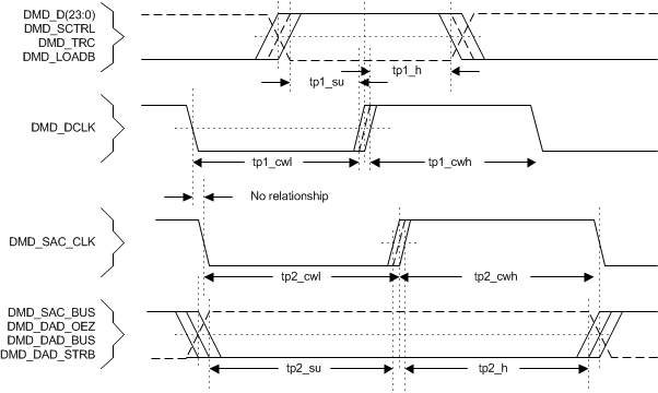 Figure 11. DMD LPDDR Interface