ZHCSC08C December 2013 – August 2015 DLPC6401
PRODUCTION DATA.
- 1 特性
- 2 应用
- 3 说明
- 4 修订历史记录
- 5 Pin Configuration and Functions
-
6 Specifications
- 6.1 Absolute Maximum Ratings
- 6.2 ESD Ratings
- 6.3 Recommended Operating Conditions
- 6.4 Thermal Information
- 6.5 Electrical Characteristics
- 6.6 Electrical Characteristics (Normal Mode)
- 6.7 System Oscillators Timing Requirements
- 6.8 Test and Reset Timing Requirements
- 6.9 JTAG Interface: I/O Boundary Scan Application Timing Requirements
- 6.10 Port 1 Input Pixel Interface Timing Requirements
- 6.11 Port 2 Input Pixel Interface (FPD-Link Compatible LVDS Input) Timing Requirements
- 6.12 Synchronous Serial Port (SSP) Interface Timing Requirements
- 6.13 Programmable Output Clocks Switching Characteristics
- 6.14 Synchronous Serial Port (SSP) Interface Switching Characteristics
- 6.15 JTAG Interface: I/O Boundary Scan Application Switching Characteristics
- 7 Detailed Description
- 8 Application and Implementation
- 9 Power Supply Recommendations
- 10Layout
- 11器件和文档支持
- 12机械、封装和可订购信息
10 Layout
10.1 Layout Guidelines
TI recommends 2-ounce copper (2.6-mil) power and ground planes in the PCB design to achieve needed thermal connectivity.
10.1.1 PCB Layout Guidelines for Internal ASIC Power
TI recommends the following guidelines to achieve desired ASIC performance relative to internal PLLs:
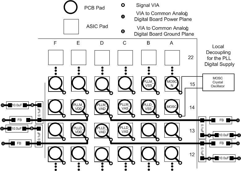
- The DLPC6401 device contains two PLLs (PLLM and PLLD), each of which has a dedicated 1.2-V digital and 1.8-V analog supply. These 1.2-V PLL pins should be individually isolated from the main 1.2-V system supply through a ferrite bead. The impedance of the ferrite bead should be much greater than that of the capacitor at frequencies where noise is expected. Specifically the impedance of the ferrite bead must be less than 0.5 Ω in the frequency range of 100 to 300 kHz and greater than 10 Ω in the frequency range >100 MHz.
- As a minimum, 1.8-V analog PLL power and ground pins should be isolated using an LC-filter with a ferrite serving as the inductor and a 0.1-µF capacitor on the ASIC side of the ferrite. TI recommends that this 1.8-V PLL power be supplied from a dedicated linear regulator and each PLL should be individually isolated from the regulator. The same ferrite recommendations described for the 1.2-V digital PLL supply apply to the 1.8-V analog PLL supplies.
- When designing the overall supply filter network, take care to ensure no resonance occurs. Particularly take care around the 1- to 2-mHz band, as this coincides with the PLL natural loop frequency.
 Figure 18. PLL Filter Layout
High-frequency decoupling is required for both 1.2-V and 1.8-V PLL supplies and should be provided as close as possible to each of the PLL supply package pins. TI recommends placing decoupling capacitors under the package on the opposite side of the board. Use high-quality, low-ESR, monolithic, surface mount capacitors. Typically 0.1 µF for each PLL supply should be sufficient. The length of a connecting trace increases the parasitic inductance of the mounting, and thus, where possible, there should be no trace, allowing the via to butt up against the land itself. Additionally, the connecting trace should be made as wide as possible. Further improvement can be made by placing vias to the side of the capacitor lands or doubling the number of vias.
The location of bulk decoupling depends on the system design. Typically, a good ceramic capacitor in the 10-µF range is adequate.
10.1.2 PCB Layout Guidelines for Quality Auto-Lock Performance
One of the most important factors in getting good performance from Auto-Lock is to design the PCB with the highest-quality signal integrity possible. TI recommends the following:
- Place the ADC chip as close to the VESA/video connectors as possible.
- Avoid crosstalk to the analog signals by keeping them away from digital signals.
- Do not place the digital ground or power planes under the analog area between the VESA connector to the ADC chip.
- Avoid crosstalk onto the RGB analog signals. Separate them from the VESA Hsync and Vsync signals.
- Analog power should not be shared with the digital power directly.
- Try to keep the trace lengths of the RGB as equal as possible.
- Use good quality (1%) termination resistors for the RGB inputs to the ADC.
- If the green channel must be connected to more than the ADC green input and ADC sync-on-green input, provide a good-quality high-impendence buffer to avoid adding noise to the green channel.
10.1.3 DMD Interface Considerations
The DMD interface is modeled after the low-power DDR memory (LPDDR) interface. To minimize power dissipation, the LPDDR interface is defined to be unterminated. This makes good PCB signal integrity management imperative. In particular, impedance control and crosstalk mitigation is critical to robust operation. LPDDR board design recommendations include 3× design rules (that is, trace spacing = 3× trace width), ±10% impedance control, and signal routing directly over a neighboring reference plane (ground or 1.9-V plane).
DMD interface performance is also a function of trace length, so even with good board design, the length of the line limits performance. The DLPC6401 device works over a very-narrow range of DMD signal routing lengths at 120 MHz only. The device provides the option to reduce the interface clock rate to facilitate a longer interface (this includes 106.7-MHz, 96-MHz, 87.7-MHz, and 80-MHz programming options). However, note that reducing the interface clock rate has the impact of increasing DMD load time, which in turn reduces image quality. Even with a clock reduction, the edge rates required to achieve the fastest clock rates still exist and cause overshoot and undershoot issues if there is excessive crosstalk, or the line is too short. Thus, ensuring positive timing margin requires attention to many factors.
As an example, DMD interface system timing margin can be calculated as follows:
Where PCB SI degradation is signal integrity degradation due to PCB effects, which include simultaneously switching output (SSO) noise, crosstalk, and inter-symbol interference (ISI). The DLPC6401 I/O timing parameters can be found in their corresponding tables. Similarly, PCB routing mismatch can be budgeted and met through controlled PCB routing. However, PCB SI degradation is not so straightforward.
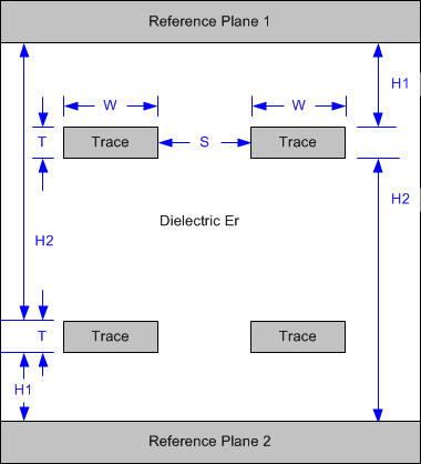
In an attempt to minimize the signal integrity analysis that would otherwise be required, the following PCB design guidelines are provided as a reference of an interconnect system that satisfies both waveform quality and timing requirements (accounting for both PCB routing mismatch and PCB SI degradation). Variation from these recommendations may also work, but should be confirmed with PCB signal integrity analysis or lab measurements.
| PCB design: | |||
| ● | Configuration: | Asymmetric dual stripline | |
| ● | Signal routing layer thickness (T): | 1.0-oz copper (1.2 mil) | |
| ● | Single-ended signal impedance controlled: | 50 Ω (±10%) | |
| ● | Differential signal impedance controlled: | 100-Ω differential (±10%) | |
| PCB Stackup: | |||
| ● | Reference plane 1 is assumed to be a ground plane for proper return path. | ||
| ● | Reference plane 2 is assumed to be the 1.9-V DMD I/O power plane or another ground plane. | ||
| ● | Dielectric FR4, (Er): | 4.3 at 1 GHz (nominal) | |
| ● | Signal trace distance to reference plane 1 (H1): | 5 mil (nominal) | |
| ● | Signal trace distance to reference plane 2 (H2): | 30.4 mil (nominal) | |
| ● | If additional routing layers are required, ensure they are adjacent to one of these reference planes | ||
 Figure 19. PCB Stackup Geometries Figure 19. PCB Stackup Geometries
|
|||
| Flex design: | |||
| ● | Configuration: | 2-layer microstrip | |
| ● | The reference plane is assumed to be a ground plane for proper return path. | ||
| ● | Vias: | Max 2 per signal | |
| ● | Single trace width: | 4 mil (min) | |
| ● | Signal routing layer thickness (T): | 0.5-oz copper (0.6 mil) | |
| ● | Single-ended signal impedance controlled: | 50 Ω (±10%) | |
Table 11. General PCB Routing (Applies to All Corresponding PCB Signal)
| PARAMETER | APPLICATION | SINGLE-ENDED SIGNALS | REQUIREMENT | UNIT |
|---|---|---|---|---|
| Line width (W)(1) | Escape routing in ball field | 4 (0.1) |
Minimum | mil (mm) |
| PCB etch data or control | 5 (0.13) |
Minimum | mil (mm) |
|
| PCB etch clocks | 7 (0.18) |
Minimum | mil (mm) |
|
| Minimum Line spacing to other signals (S) |
Escape routing in ball field | 4 (0.1) |
Minimum | mil (mm) |
| PCB etch data or control | 2× the line width(2) | Minimum | mil (mm) |
|
| PCB etch clocks | 3x the line width | Minimum | mil (mm) |
Table 12. DMD I/F, PCB Interconnect Length Matching Requirements(1)(2)
| SIGNAL GROUP LENGTH MATCHING | ||||
|---|---|---|---|---|
| I/F | SIGNAL GROUP | REFERENCE SIGNAL | MAX MISMATCH | UNIT |
| DMD (DDR) | DMD_TRC, DMD_SCTRL, DMD_LOADB DMD_D(23:0) |
DMD_DCLK | ±200 (±5.08) |
mil (mm) |
| DMD (SDR) | DMD_SAC_BUS, DMD_DAD_OEZ, DMD_DAD_STRB, DMD_DAD_BUS |
DMD_SAC_CLK | ±200 (± 5.08) |
mil (mm) |
Table 13. DMD I/F, PCB(3) Interconnect Min and Max Length Limitations (Note Operating Frequency Dependencies)(4)
| BUS | SIGNAL GROUP | SIGNAL ROUTING LENGTH | UNIT | ||||
|---|---|---|---|---|---|---|---|
| MIN(1) | MAX(1)(2) | ||||||
| 120 MHz | 106.7 MHz | 96 MHz | 87.7 MHz | ||||
| DMD (DDR) | DMD_DCLK, DMD_TRC, DMD_SCTRL, DMD_LOADB DMD_D(23:0) |
2480 (63) |
2953 (75) |
3465 (88) |
3937 (100) |
3937 (100) |
mil (mm) |
| DMD (SDR) | DMD_SAC_CLK, DMD_SAC_BUS, DMD_DAD_OEZ, DMD_DAD_STRB, DMD_DAD_BUS |
512 (13) |
5906 (150) |
mil (mm) |
|||
spacer
- Number of layer changes:
- Minimize layer changes
- Stubs:
- Stubs should be avoided
| Termination requirements: | ||
| DMD DDR data: | Specifically: DMD_D(23-0) External [5-Ω] series termination (at the transmitter) |
|
| DMD DDR clock | Specifically: DMD_DCLK External [5-Ω] series termination |
|
| DMD TRC, SCTRL, load: | Specifically: DMD_TRC, DMD_SCTRL, DMD_LOADB External [5-Ω] series termination (at the transmitter) |
|
| DMD SAC and miscellaneous control: | Specifically: DMD_SAC_CLK, DMD_SAC_BUS, DMD_DAD_STRB, DMD_DAD_BUS External [5-Ω] series termination (at the transmitter) |
|
| DAD output enable: | Specifically: DMD_DAD_OEZ External [0-Ω] series termination Instead this signal must be externally pulled-up to VDD_DMD through a 30- to 51-kΩ resistor. |
|
However, note that both the DLPC6401 output timing parameters and the DMD input timing parameters include timing budget to account for their respective internal package routing skew. Thus, additional system margin can be attained by comprehending the package variations and compensating for them in the PCB layout. To increase system timing margin, TI recommends that DLPC6401 package variation be compensated for (by signal group), but it may not be desirable to compensate for DMD package skew. Because, each DMD has a different skew profile making the PCB layout DMD specific. Thus, if an OEM wants to use a common PCB design for different DMDs, TI recommends that either the DMD package skew variation not be compensated for on the PCB or the package lengths for all applicable DMDs be considered. Table 14 provides the DLPC6401 package output delay at the package ball for each DMD I/F signal. DMD internal routing skew data is contained in the DMD data sheet.
Table 14. DLPC6401 DMD I/F Package Routing Length
| SIGNAL | TOTAL DELAY (ps) | PACKAGE BALL | SIGNAL | TOTAL DELAY (ps) | PACKAGE BALL |
|---|---|---|---|---|---|
| DMD_D0 | 25.9 | A8 | DMD_D14 | 19 | B12 |
| DMD_D1 | 19.6 | B8 | DMD_D15 | 11.7 | C12 |
| DMD_D2 | 13.4 | C8 | DMD_D16 | 4.7 | D12 |
| DMD_D3 | 7.4 | D8 | DMD_D17 | 21.5 | B7 |
| DMD_D4 | 18.1 | B11 | DMD_D18 | 24.8 | A10 |
| DMD_D5 | 11.1 | C11 | DMD_D19 | 8.3 | D7 |
| DMD_D6 | 4.4 | D11 | DMD_D20 | 23.9 | B6 |
| DMD_D7 | 0 | E11 | DMD_D21 | 1.6 | E9 |
| DMD_D8 | 14.8 | C7 | DMD_D22 | 10.7 | C10 |
| DMD_D9 | 18.4 | B10 | DMD_D23 | 16.7 | C6 |
| DMD_D10 | 6.4 | E7 | DMD_DCLK | 24.8 | A9 |
| DMD_D11 | 4.8 | D10 | DMD_LOADB | 18 | B9 |
| DMD_D12 | 29.8 | A6 | DMD_SCTRL | 11.4 | C9 |
| DMD_D13 | 25.7 | A12 | DMD_TRC | 4.6 | D9 |
10.1.4 General Handling Guidelines for Unused CMOS-Type Pins
To avoid potentially damaging current caused by floating CMOS input-only pins, TI recommends that unused ASIC input pins be tied through a pullup resistor to its associated power supply or a pulldown to ground. For ASIC inputs with an internal pullup or pulldown resistors, it is unnecessary to add an external pullup or pulldown, unless specifically recommended. Note that internal pullup and pulldown resistors are weak and should not be expected to drive the external line.
Unused output-only pins can be left open.
When possible, TI recommends that unused bidirectional I/O pins be configured to their output state such that the pin can be left open. If this control is not available and the pins may become an input, then they should be pulled-up (or pulled-down) using an appropriate resistor.
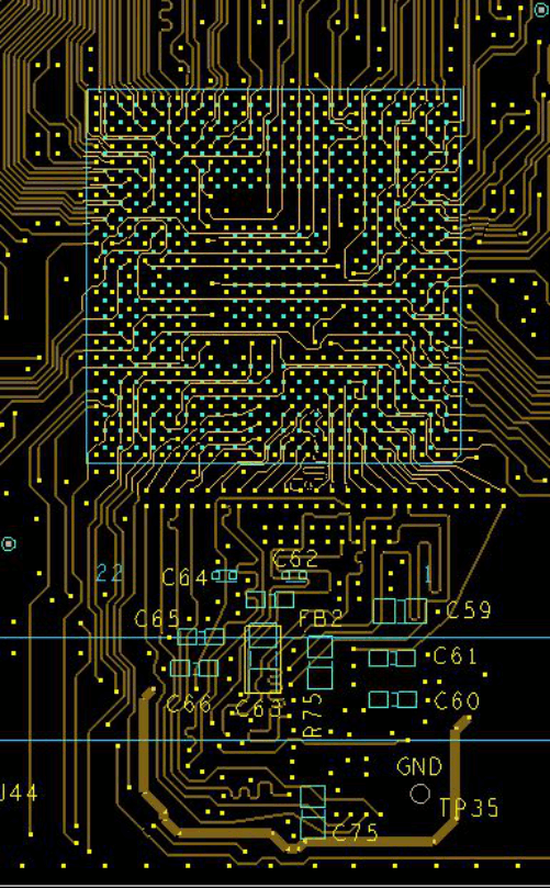
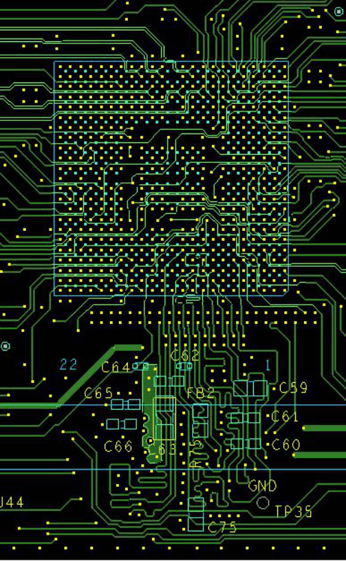
10.2 Layout Example
 Figure 20. Layer 3
 Figure 21. Layer 4
10.3 Thermal Considerations
The underlying thermal limitation for the DLPC6401 device is that the maximum operating junction temperature (TJ) not be exceeded (this is defined in the Recommended Operating Conditions). This temperature depends on operating ambient temperature, airflow, PCB design (including the component layout density and the amount of copper used), power dissipation of the DLPC6401 device, and power dissipation of surrounding components. The DLPC6401 package is designed primarily to extract heat through the power and ground planes of the PCB, thus copper content and airflow over the PCB are important factors.
The recommended maximum operating ambient temperature (TA) is provided primarily as a design target and is based on maximum DLPC6401 power dissipation and RθJA at 1 m/s of forced airflow, where RθJA is the thermal resistance of the package as measured using a JEDEC-defined standard test PCB. This JEDEC test PCB is not necessarily representative of the DLPC6401 PCB, and thus the reported thermal resistance may not be accurate in the actual product application. Although the actual thermal resistance may be different, it is the best information available during the design phase to estimate thermal performance. However, after the PCB is designed and the product is built, TI highly recommends that thermal performance be measured and validated.
To do this, the top-center case temperature should be measured under the worst-case product scenario (maximum power dissipation, maximum voltage, and maximum ambient temperature) and validated not to exceed the maximum recommended case temperature (TC). This specification is based on the measured φJT for the DLPC6401 package and provides a relatively accurate correlation to junction temperature. Take care when measuring this case temperature to prevent accidental cooling of the package surface. TI recommends a small (approximately 40-gauge) thermocouple. The bead and the thermocouple wire should contact the top of the package and be covered with a minimal amount of thermally-conductive epoxy. The wires should be routed closely along the package and the board surface to avoid cooling the bead through the wires.