SCAS882E June 2009 – October 2016 CDCE62002
PRODUCTION DATA.
- 1 Features
- 2 Applications
- 3 Description
- 4 Revision History
- 5 Description (continued)
- 6 Pin Configuration and Functions
- 7 Specifications
- 8 Parameter Measurement Information
-
9 Detailed Description
- 9.1 Overview
- 9.2 Functional Block Diagrams
- 9.3
Feature Description
- 9.3.1 Phase Noise Analysis
- 9.3.2 Output-to-Output Isolationthe OUTPUT TO OUTPUT ISOLATION section
- 9.3.3 Device Control
- 9.3.4 External Control Pins
- 9.3.5 Input Block
- 9.3.6 Lock Detect
- 9.3.7 Crystal Input Interface
- 9.3.8 VCO Calibration
- 9.3.9 Start-Up Time Estimation
- 9.4 Device Functional Modes
- 9.5 Programming
- 9.6 Register Maps
- 10Power Supply Recommendations
- 11Layout
- 12Device and Documentation Support
- 13Mechanical, Packaging, and Orderable Information
7 Specifications
7.1 Absolute Maximum Ratings
over operating free-air temperature range (unless otherwise noted) (1)| MIN | MAX | UNIT | ||
|---|---|---|---|---|
| Supply voltage VCC(2) | –0.5 | V | ||
| Input voltage, VI (3) | –0.5 | V | ||
| Output voltage, VO (3) | –0.5 | V | ||
| Input current (VI < 0, VI > VCC) | ±20 | mA | ||
| Output current for LVPECL/LVCMOS Outputs (0 < VO < VCC) | ±50 | mA | ||
| TJ | Junction temperature | 125 | °C | |
| Tstg | Storage temperature | –65 | 150 | °C |
(1) Stresses beyond those listed under Absolute Maximum Ratings may cause permanent damage to the device. These are stress ratings only and functional operation of the device at these or any other conditions beyond those indicated under Recommended Operating Conditions is not implied. Exposure to absolute–maximum–rated conditions for extended periods may affect device reliability.
(2) All supply voltages have to be supplied simultaneously.
(3) The input and output negative voltage ratings may be exceeded if the input and output clamp-current ratings are observed.
7.2 Thermal Information
| THERMAL METRIC(1) | CDCE62002 | UNIT | ||
|---|---|---|---|---|
| QFN (RGZ) | ||||
| 32 PINS | ||||
| RθJA | Junction-to-ambient thermal resistance (JEDEC Compliant Board - 3×3 vias on pad) | 0-lfm Airflow | 35 | °C/W |
| 200-lfm Airflow | 28.3 | |||
| 400-lfm Airflow | 27.2 | |||
| RθJP | Junction-to-pad | 1.13 | °C/W | |
(1) For more information about traditional and new thermal metrics, see the Semiconductor and IC Package Thermal Metrics application report.
7.3 Electrical Characteristics
recommended operating conditions for the CDCE62002 Device for under the specified Industrial temperature range of –40°C to 85°C| PARAMETER | TEST CONDITIONS | MIN | TYP(1) | MAX | UNIT | ||
|---|---|---|---|---|---|---|---|
| POWER SUPPLY | |||||||
| Supply voltage, VCC_OUT, VCC_PLLDIV, VCC_PLLD, VCC_IN, and VCC_AUX | 3 | 3.3 | 3.6 | V | |||
| Analog supply voltage, VCC_PLLA, & VCC_VCO | 3 | 3.3 | 3.6 | V | |||
| PLVPECL | REF at 30.72 MHz, outputs are LVPECL | Output 1 = 491.52 MHz
Output 2 = 245.76 MHz In case of LVCMOS Outputs (1) = 245.76MHz |
850 | mW | |||
| PLVDS | REF at 30.72 MHz, outputs are LVDS | 750 | mW | ||||
| PLVCMOS | REF at 30.72 MHz, outputs are LVCMOS | 800 | mW | ||||
| POFF | REF at 30.72 MHz | Outputs are disabled | 450 | mW | |||
| PPD | Device is powered down | 40 | mW | ||||
| DIFFERENTIAL INPUT MODE (REF_IN) | |||||||
| Differental Input amplitude, (VIN+ – VIN–) | 0.1 | 1.3 | V | ||||
| Common-mode input voltage, VIC | 1.0 | VCC–03 | V | ||||
| IIH | Differential input current high (no internal termination) | VI = VCC, VCC = 3.6 V |
20 | μA | |||
| IIL | Differential input current low (no internal termination) | VI = 0 V, VCC = 3.6 V |
–20 | μA | |||
| Input Capacitance on REF_IN | 3 | pF | |||||
| CRYSTAL INPUT SPECIFICATIONS | |||||||
| On-chip load capacitance | 8 | 10 | pF | ||||
| Equivalent Series Resistance (ESR) | 50 | Ω | |||||
| LVCMOS INPUT MODE (SPI_CLK,SPI_MOSI,SPI_LE,PD, REF_IN) | |||||||
| VIL | Low-level input voltage LVCMOS | 0 | 0.3 VCC | V | |||
| VIH | High-level input voltage LVCMOS | 0.7 VCC | VCC | V | |||
| VIK | LVCMOS input clamp voltage | VCC = 3 V, II = –18 mA | –1.2 | V | |||
| IIH | LVCMOS input current VI = | VCC, VCC = 3.6 V | 20 | μA | |||
| IIL | LVCMOS input (Except REF_IN) | VI = 0 V, VCC = 3.6 V | –10 | –40 | μA | ||
| IIL | LVCMOS input (REF_IN) | VI = 0 V, VCC = 3.6 V | –10 | 10 | μA | ||
| CI | Input capacitance (LVCMOS signals) | VI = 0 V or VCC = 3 | 3 | pF | |||
| SPI OUTPUT (MISO) / PLL_LOCK | |||||||
| IOH | High-level output current | VCC = 3.3 V, | VO = 1.65 V | –30 | mA | ||
| IOL | Low-level output current | VCC = 3.3 V, | VO = 1.65 V | 33 | mA | ||
| VOH | High-level output voltage for LVCMOS outputs | VCC = 3 V, | IOH = –100 μA | VCC–0.5 | V | ||
| VOL | Low-level output voltage for LVCMOS outputs | VCC = 3 V, | IOH = 100 μA | 0.3 | V | ||
| CO | Output capacitance o MISO | VCC = 3.3 V; VO = 0 V or VCC | 3 | pF | |||
| IOZH | 3-state output current | VO = VCC, VO = 0 V | 5 | μA | |||
| IOZL | –5 | μA | |||||
| EEPROM | |||||||
| EEcyc | Programming cycle of EEPROM | 100 | 1000 | Cycles | |||
| EEret | Data retention | 10 | Years | ||||
| VBB ( INPUT BUFFER INTERNAL TERMINATION VOLTAGE REFERENCE) | |||||||
| VBB | Input termination voltage | IBB = –0.2 mA, depending on the setting | 1.2 | 1.9 | V | ||
| INPUT BUFFERS INTERNAL TERMINATION RESISTORS (REF_IN) | |||||||
| Termination resistance | Single-ended | 5 | kΩ | ||||
| PHASE DETECTOR | |||||||
| fCPmax | Charge pump frequency | 0.04 | 40 | MHz | |||
| LVCMOS | |||||||
| fclk | Output frequency, see Figure 7 | Load = 5 pF to GND | 250 | MHz | |||
| VOH | High-level output voltage for LVCMOS outputs | VCC = min to max | IOH = –100 μA | VCC–0.5 | V | ||
| VOL | Low-level output voltage for LVCMOS outputs | VCC = min to max | IOL = 100 μA | 0.3 | V | ||
| IOH | High-level output current | VCC = 3.3 V | VO = 1.65 V | –30 | mA | ||
| IOL | Low-level output current | VCC = 3.3 V | VO = 1.65 V | 33 | mA | ||
| tsko | Skew, output to output For Y0 to Y1 | Both outputs set at 122.88 MHz, reference = 30.72 MHz |
75 | ps | |||
| CO | Output capacitance on Y0 to Y1 | VCC = 3.3 V; VO = 0 V or VCC | 5 | pF | |||
| IOZH | Tristate LVCMOS output current | VO = VCC | 5 | μA | |||
| IOZL | Tristate LVCMOS output current | VO = 0 V | -5 | μA | |||
| IOPDH | Power-down output current | VO = VCC | 25 | μA | |||
| IOPDL | Power-down output current | VO = 0 V | 5 | μA | |||
| Duty cycle | LVCMOS | 45% | 55% | ||||
| tslew-rate | Output rise/fall slew rate | 3.6 | 5.2 | V/ns | |||
| LVDS OUTPUT | |||||||
| fclk | Output frequency | Configuration load (see Figure 8) | 0 | 800 | MHz | ||
| |VOD| | Differential output voltage | RL = 100 Ω | 270 | 550 | mV | ||
| ΔVOD | LVDS VOD magnitude change | 50 | mV | ||||
| VOS | Offset voltage | –40°C to 85°C | 1.24 | V | |||
| ΔVOS | VOS magnitude change | 40 | mV | ||||
| Short-circuit Vout+ to ground | VOUT = 0 | 27 | mA | ||||
| Short-cicuit Vout- to ground | VOUT = 0 | 27 | mA | ||||
| tsk(o) | Skew, output to output For Y0 to Y1 | Both outputs set at 122.88 MHz reference = 30.72 MHz |
10 | ps | |||
| CO | Output capacitance on Y0 to Y1 | VCC = 3.3 V; VO = 0 V or VCC | 5 | pF | |||
| IOPDH | Power-down output current | VO = VCC | 25 | μA | |||
| IOPDL | Power-down output current | VO = 0 V | 5 | μA | |||
| Duty cycle | 45% | 55% | |||||
| tr / tf | Rise and fall time | 20% to 80% of VOPP | 110 | 160 | 190 | ps | |
| LVCMOS-TO-LVDS | |||||||
| tskP_C | Output skew between LVCMOS and LVDS outputs | VCC/2 to crosspoint | 1.4 | 1.7 | 2.0 | ns | |
| LVPECL OUTPUT | |||||||
| fclk | Output frequency | Configuration load (see Figure 9 and Figure 10) | 0 | 1175 | MHz | ||
| VOH | LVPECL high-level output voltage | Load | VCC –1.1 | VCC –0.88 | V | ||
| VOL | LVPECL low-level output voltage | Load | VCC –2.02 | VCC –1.48 | V | ||
| |VOD| | Differential output voltage | 510 | 870 | mV | |||
| tsko | Skew, output to output For Y0 to Y1 | Both outputs set at 122.88 MHz | 15 | ps | |||
| CO | Output capacitance on Y0 to Y1 | VCC = 3.3 V; VO = 0 V or VCC | 5 | pF | |||
| IOPDH | Power-down output current | VO = VCC | 25 | μA | |||
| IOPDL | Power-down output current | VO = 0 V | 5 | μA | |||
| Duty cycle | 45% | 55% | |||||
| tr / tf | Rise and fall time | 20% to 80% of VOPP | 55 | 75 | 135 | ps | |
| LVDS-TO- LVPECL | |||||||
| tskP_C | Output skew between LVDS and LVPECL outputs | Crosspoint to Crosspoint | 130 | 200 | 280 | ps | |
| LVCMOS-TO- LVPECL | |||||||
| tskP_C | Output skew between LVCMOS and LVPECL outputs | VCC/2 to Crosspoint | 1.6 | 1.8 | 2.2 | ns | |
| LVPECL Hi-PERFORMANCE OUTPUT | |||||||
| VOH | LVPECL high-level output voltage | Load | VCC –1.11 | VCC –0.91 | V | ||
| VOL | LVPECL low-level output voltage | Load | VCC –2.06 | VCC –1.84 | V | ||
| |VOD| | Differential output voltage | 670 | 950 | mV | |||
| tr / tf | Rise and fall time | 20% to 80% of VOPP | 55 | 75 | 135 | ps | |
(1) All typical values are at VCC = 3.3 V, temperature = 25°C.
7.4 Timing Requirements
over recommended ranges of supply voltage, load and operating free-air temperature range (unless otherwise noted)7.5 SPI Bus Timing Characteristics
| PARAMETER | MIN | TYP | MAX | UNIT | |
|---|---|---|---|---|---|
| fClock | Clock frequency for the SPI_CLK | 20 | MHz | ||
| t1 | SPI_LE to SPI_CLK setup time | 10 | ns | ||
| t2 | SPI_MOSI to SPI_CLK setup time | 10 | ns | ||
| t3 | SPI_MOSI to SPI_CLK hold time | 10 | ns | ||
| t4 | SPI_CLK high duration | 25 | ns | ||
| t5 | SPI_CLK low duration | 25 | ns | ||
| t6 | SPI_CLK to SPI_LE hold time | 10 | ns | ||
| t7 | SPI_LE pulse width | 20 | ns | ||
| t8 | SPI_CLK to MISO data valid | 10 | ns | ||
| t9 | SPI_LE to SPI_MISO data valid | 10 | ns | ||
 Figure 1. Timing Diagram for SPI Write Command
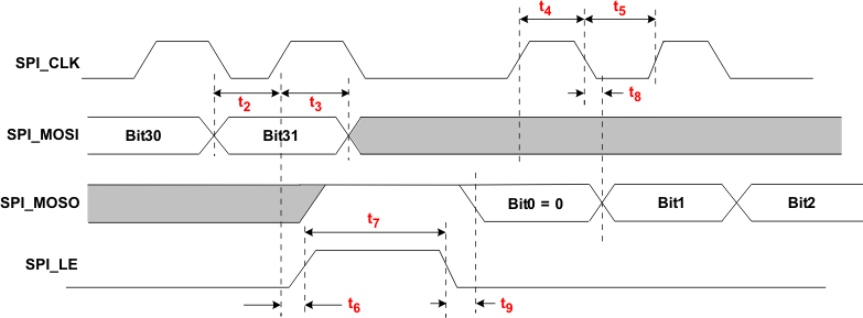 Figure 2. Timing Diagram for SPI Read Command
7.6 Typical Characteristics
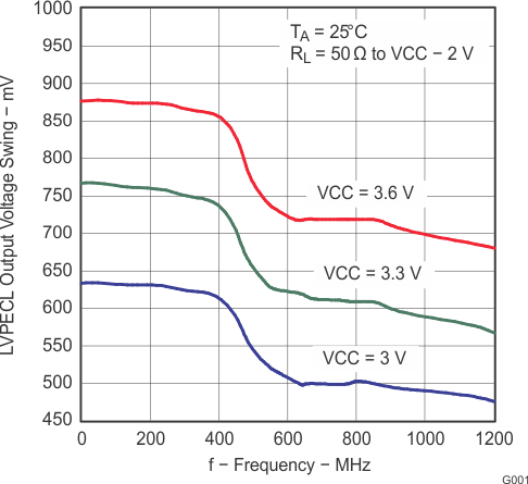 Figure 3. LVPECL Output Voltage Swing vs Frequency
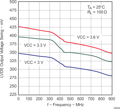 Figure 5. LVDS Output Voltage Swing vs Frequency
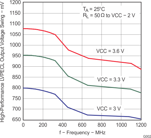 Figure 4. High-Performance LVPECL Output Voltage Swing vs Frequency
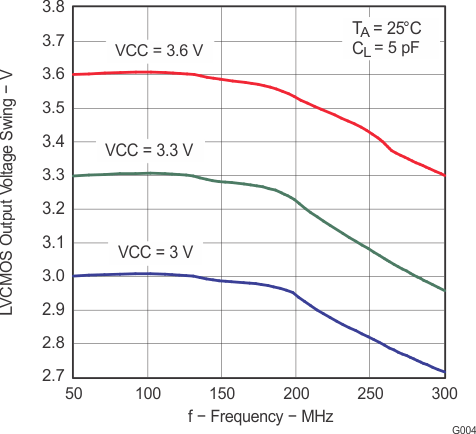 Figure 6. LVCMOS Output Voltage Swing vs Frequency