SCAS882E June 2009 – October 2016 CDCE62002
PRODUCTION DATA.
- 1 Features
- 2 Applications
- 3 Description
- 4 Revision History
- 5 Description (continued)
- 6 Pin Configuration and Functions
- 7 Specifications
- 8 Parameter Measurement Information
-
9 Detailed Description
- 9.1 Overview
- 9.2 Functional Block Diagrams
- 9.3
Feature Description
- 9.3.1 Phase Noise Analysis
- 9.3.2 Output-to-Output Isolationthe OUTPUT TO OUTPUT ISOLATION section
- 9.3.3 Device Control
- 9.3.4 External Control Pins
- 9.3.5 Input Block
- 9.3.6 Lock Detect
- 9.3.7 Crystal Input Interface
- 9.3.8 VCO Calibration
- 9.3.9 Start-Up Time Estimation
- 9.4 Device Functional Modes
- 9.5 Programming
- 9.6 Register Maps
- 10Power Supply Recommendations
- 11Layout
- 12Device and Documentation Support
- 13Mechanical, Packaging, and Orderable Information
10 Power Supply Recommendations
The CDCE62002 is a high-performance device; therefore pay careful attention to device configuration and printed-circuit board layout with respect to power consumption. Table 20 provides the power consumption for the individual blocks within the CDCE62002. To estimate total power consumption, calculate the sum of the products of the number of blocks used and the power dissipated of each corresponding block.
Table 20. CDCE62002 Power Consumption
| INTERNAL BLOCK (Power at 3.3 V) |
POWER DISSIPATED PER BLOCK (mW) |
NUMBER OF BLOCKS PER DEVICE |
|---|---|---|
| Input circuit | 32 | 1 |
| PLL and VCO core | 333 | 1 |
| Output divider | 92 | 2 |
| Output buffer ( LVPECL) | 150 | 2 |
| Output buffer (LVDS) | 95 | 2 |
| Output buffer (LVCMOS) | 62 | 4 |
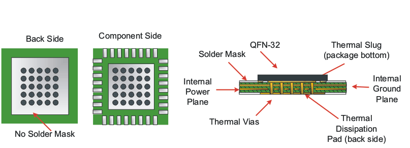
This power estimate determines the degree of thermal management required for a specific design. Observing good thermal layout practices enables the thermal pad on the backside of the 32-pin VQFN package to provide a good thermal path between the die contained within the package and the ambient air. This thermal pad also serves as the ground connection the device; therefore, a low inductance connection to the ground plane is essential.
 Figure 37. CDCE62002 Recommended PCB Layout