SCAS882E June 2009 – October 2016 CDCE62002
PRODUCTION DATA.
- 1 Features
- 2 Applications
- 3 Description
- 4 Revision History
- 5 Description (continued)
- 6 Pin Configuration and Functions
- 7 Specifications
- 8 Parameter Measurement Information
-
9 Detailed Description
- 9.1 Overview
- 9.2 Functional Block Diagrams
- 9.3
Feature Description
- 9.3.1 Phase Noise Analysis
- 9.3.2 Output-to-Output Isolationthe OUTPUT TO OUTPUT ISOLATION section
- 9.3.3 Device Control
- 9.3.4 External Control Pins
- 9.3.5 Input Block
- 9.3.6 Lock Detect
- 9.3.7 Crystal Input Interface
- 9.3.8 VCO Calibration
- 9.3.9 Start-Up Time Estimation
- 9.4 Device Functional Modes
- 9.5 Programming
- 9.6 Register Maps
- 10Power Supply Recommendations
- 11Layout
- 12Device and Documentation Support
- 13Mechanical, Packaging, and Orderable Information
9 Detailed Description
9.1 Overview
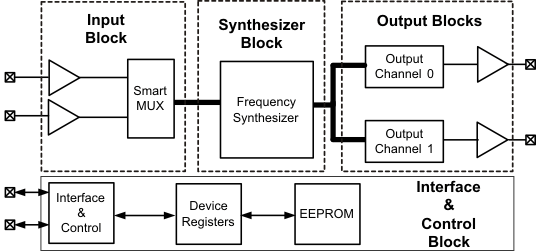
The CDCE62002 comprises of four primary blocks: the interface and control block, the input block, the output block, and the synthesizer block. To determine which settings are appropriate for any specific combination of input and output frequencies, a basic understanding of these blocks is required. The interface and control block determines the state of the CDCE62002 at power up based on the contents of the onboard EEPROM. In addition to the EEPROM, the SPI port is available to configure the CDCE62002 by writing directly to the device registers after power up. The input block selects which of the two input ports is available for use by the synthesizer block. The output block provides two separate clock channels that are fully programmable. The synthesizer block multiplies and filters the input clock selected by the input block.
NOTE
This section of the data sheet provides a high-level description of the features of the CDCE62002 for purpose of understanding its capabilities. For a complete description of device registers and I/O, refer to the Device Configuration section.
9.2 Functional Block Diagrams
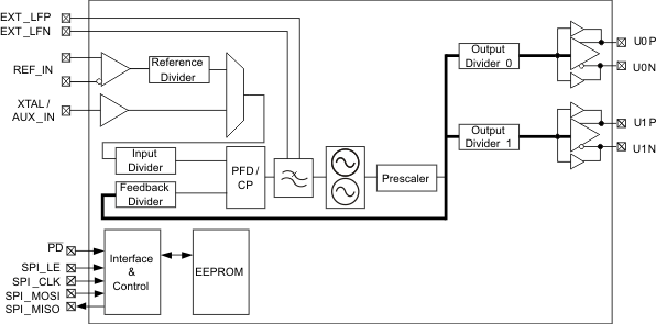 Figure 11. CDCE62002 Block Diagram
9.2.1 Interface and Control Block
The CDCE62002 is a highly flexible and configurable architecture and as such contains a number of registers so that the user may specify device operation. The contents of three 28-bit wide registers implemented in static RAM determine device configuration at all times. On power up, the CDCE62002 copies the contents of the EEPROM into the RAM and the device begins operation based on the default configuration stored in the EEPROM. Systems that do not have a host system to communicate with the CDCE62002 use this method for device configuration.After power up, the host system may overwrite the contents of the RAM through the SPI (Serial Peripheral Interface) port. This enables the configuration and reconfiguration of the CDCE62002 during system operation. Finally, the device offers the ability to copy the contents of the RAM into EEPROM
9.2.2 Input Block
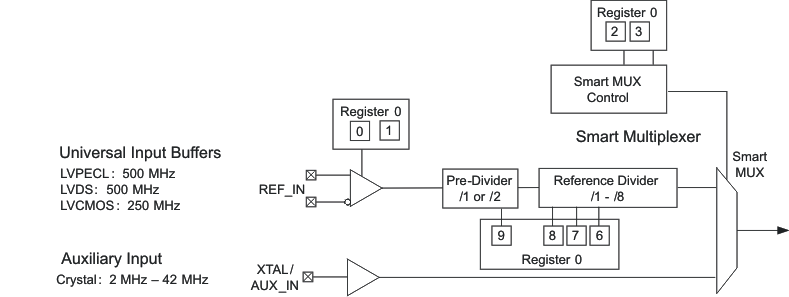
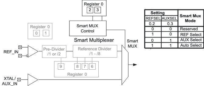
The input block includes one universal input buffer and an auxiliary input. The input block buffers the incoming signals and facilitates signal routing to the Internal synthesizer block through the smart multiplexer (called the smart MUX). The CDCE62002 can divide the REF_IN signal through the dividers present on the inputs of the first stage of the smart MUX.
 Figure 13. CDCE62002 Input Block
9.2.3 Output Block
Both identical output blocks incorporate a clock divider module (CDM), and a universal output buffer. If an individual clock output channel is not used, then the user should disable the output buffer for the unused channel to save device power. Each channel includes 4-bit in register 0 to control the divide ratio. The output divider supports divide ratios from divide of 1 (bypass the divider) 2, 3, 4, 5, 8, 10, 12, 16, 20, 24, and 32.
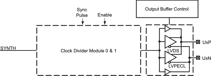 Figure 14. CDCE62002 Output Block
9.2.4 Synthesizer Block
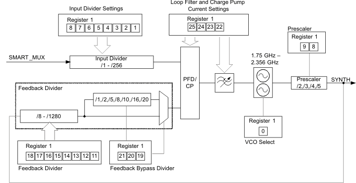
Figure 15 presents a high-level overview of the synthesizer block on the CDCE62002. This block contains the phase-locked loop, internal loop filter, and dual voltage-controlled oscillators. Only one VCO is selected at a time. The loop is closed after a prescaler divider that feeds the output stage the feedback divider.
 Figure 15. CDCE62002 Synthesizer Block
9.2.5 Computing the Output Frequency
Figure 16 presents the block diagram of the CDCE62002 synthesizer highlighting the clock path for a single output. It also identifies the following regions containing dividers comprising the complete clock path:
- R: Is the Reference divider values.
- O: The output divider value (see Output Block for more details)
- I: The input divider value (see Synthesizer Block for more details)
- P: The Prescaler divider value (see Synthesizer Block of more details)
- F: The cumulative divider value of all dividers falling within the feedback divider (see Synthesizer Block for more details)
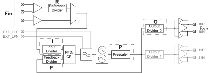 Figure 16. CDCE62002 Clock Path – Synthesizer
With respect to Figure 16, any output frequency generated by the CDCE62002 relates to the input frequency connected to the Synthesizer Block by Equation 1:

Equation 1 holds true subject to the constraints in Equation 2:

And the comparison frequency FCOMP,
40.0 kHz ≤ FCOMP ≤ 40 MHz
Where:

When AUX_IN is selected as the input, R can be set to 1 in Equation 1 and Equation 3.
9.3 Feature Description
9.3.1 Phase Noise Analysis
Table 1. Phase Noise for 30.72-MHz External Reference
Table 2. Phase Noise for 25-MHz Crystal Reference
| Phase Noise Specifications under following configuration: VCO = 2000.00 MHz, AUX_IN-REF = 25.00 MHz, PFD Frequency = 25.00 MHz, Charge Pump Current = 1.5-mA Loop BW = 400 kHz 3.3V and 25°C. |
||||
|---|---|---|---|---|
| PHASE NOISE AT | LVPECL-HP 500.00 MHz |
LVDS 250.00 MHz |
LVCMOS 125.00 MHz |
UNIT |
| 10Hz | –72 | –72 | –79 | dBc/Hz |
| 100Hz | –97 | –97 | –103 | dBc/Hz |
| 1kHz | –111 | –111 | –118 | dBc/Hz |
| 10kHz | –120 | –120 | –126 | dBc/Hz |
| 100kHz | –124 | –124 | –130 | dBc/Hz |
| 1MHz | –136 | –136 | –142 | dBc/Hz |
| 10MHz | –147 | –147 | –151 | dBc/Hz |
| 20MHz | –148 | –148 | –151 | dBc/Hz |
| Jitter(RMS) 10k~20MHz | 426 | 426 | 443 | fs |
9.3.2 Output-to-Output Isolation
Table 3. Output-to-Output Isolation
| WORST SPUR | UNIT | |||
|---|---|---|---|---|
| The Output to Output Isolation was tested at 3.3-V supply and 25°C ambient temperature (Default Configuration): | ||||
| Output 1 | Measured Channel | In LVDS Signaling at 125 MHz | –70 | dB |
| Output 0 | Aggressor Channel | LVPECL 156.25 MHz | ||
9.3.3 Device Control
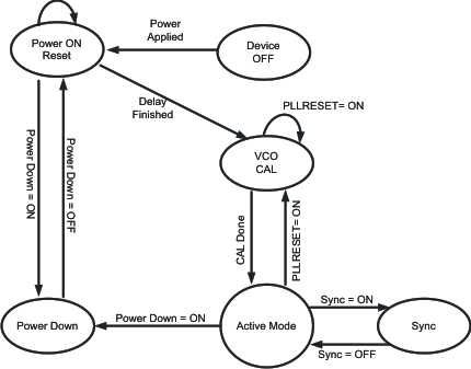
Figure 17 provides a conceptual explanation of the CDCE62002 Device operation. Table 4 defines how the device behaves in each of the operational states.
Table 4. CDCE62002 Device State Definitions
9.3.4 External Control Pins
Power Down (PD)
When pulled LOW, PD activates the power-down state which shuts down all hardware and resets the device. Restoring PD high will cause the CDCE62002 to exit the power-down state. This causes the device to behave as if it has been powered up including copying the EEPROM contents into RAM. PD pin also has a shadowed PD bit residing in Register 2 Bit 7. When asserted Low it puts the device in power-down mode, but it does not load the EEPROM when the bits is disserted.
NOTE
The SPI_LE signal has to be high in order for the EEPROM to load correctly into RAM on the Rising edge of PD Pin.
9.3.4.1 Factory Default Programming
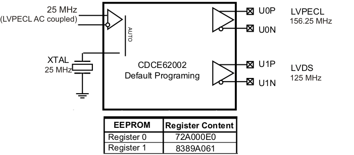
The CDCE62002 is factory pre-programmed to work with 25-MHz input from the reference input or from the auxiliary input with auto switching enabled. An internal PFD of 6.25 MHz and about 400-KHz loop bandwidth. Output 0 is pre-programmed as an LVPECL driver to output 156.25 MHz and output 1 is pre-programmed as LVDS driver to output 125 MHz.
9.3.5 Input Block
The input block includes one universal input buffers, an auxiliary input, and a smart multiplexer.
The CDCE62002 provides a reference divider that divides the clock exiting reference (REF_IN) input buffer.
Table 5. CDCE62002 Reference Divider Settings
| REFERENCE DIVIDER | TOTAL DIVIDE RATIO |
||||
|---|---|---|---|---|---|
| BIT NAME → | REFDIVIDE3 | REFDIVIDE2 | REFDIVIDE1 | REFDIVIDE0 | |
| REGISTER BIT → | 0.9 | 0.8 | 0.7 | 0.6 | |
| 0 | 0 | 0 | 0 | /1 | |
| 0 | 0 | 0 | 1 | /2 | |
| 0 | 0 | 1 | 0 | /3 | |
| 0 | 0 | 1 | 1 | /4 | |
| 0 | 1 | 0 | 0 | /5 | |
| 0 | 1 | 0 | 1 | /6 | |
| 0 | 1 | 1 | 0 | /7 | |
| 0 | 1 | 1 | 1 | /8 | |
| 1 | 0 | 0 | 0 | /2 | |
| 1 | 0 | 0 | 1 | /4 | |
| 1 | 0 | 1 | 0 | /6 | |
| 1 | 0 | 1 | 1 | /8 | |
| 1 | 1 | 0 | 0 | /10 | |
| 1 | 1 | 0 | 1 | /12 | |
| 1 | 1 | 1 | 0 | /14 | |
| 1 | 1 | 1 | 1 | /16 | |
9.3.5.1 Reference Input Buffer
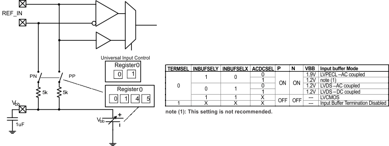
Figure 20 shows the key elements of a universal input buffer (UIB). A UIB supports multiple formats along with different termination and coupling schemes. The CDCE62002 implements the UIB by including onboard switched termination, a programmable bias voltage generator, and a multiplexer. The CDCE62002 provides a high degree of configurability on the UIB to facilitate most existing clock input formats. REF_IN only provides biasing internally. TI recommends terminating it externally if needed.
9.3.5.2 Smart Multiplexer Dividers
In auto select mode the smart Mux switches automatically between reference input and auxiliary input with a preference to the reference input. In order for the smart MUX to function correctly the frequency after the reference divider and the auxiliary input signal frequency should be within 20% of each other or one of them should be zero or ground. In REF select mode, TI recommends connecting AUX_IN to GND with a 1-k pulldown resistor. In AUX Select mode, TI recommends pulling the REF_INp high and REF_INn low with a 1-k resistor each.
9.3.5.3 Auxiliary Input Port
The auxiliary input on the CDCE62002 is designed to connect to an AT-Cut Crystal with a total load capacitance of 8 pF to 10 pF. One side of the crystal connects to ground while the other side connects to the auxiliary input of the device. The circuit accepts crystals from 2 to 42 MHz. See the Crystal Input Interface section for crystal load selection.
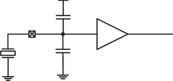 Figure 22. CDCE62002 Auxiliary Input Port
9.3.5.4 Output Block
The output block includes two identical output channels. Each output channel comprises of a clock divider module, and a universal output buffer as shown in Figure 23.
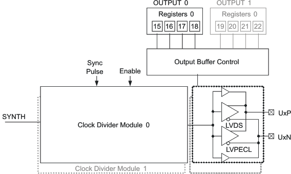 Figure 23. CDCE62002 Output Channel
Table 6. CDCE62002 Output Divider Settings
| OUTPUT DIVIDERS SETTING | DIVIDE RATIO | ||||
|---|---|---|---|---|---|
| DIVIDER 0 → | 0.18 | 0.17 | 0.16 | 0.15 | |
| DIVIDER 1 → | 0.22 | 0.21 | 0.20 | 0.19 | |
| 0 | 0 | 0 | 0 | Disabled | |
| 0 | 0 | 0 | 1 | /1 | |
| 0 | 0 | 1 | 0 | /2 | |
| 0 | 0 | 1 | 1 | /3 | |
| 0 | 1 | 0 | 0 | /4 | |
| 0 | 1 | 0 | 1 | /5 | |
| 0 | 1 | 1 | 0 | /6 | |
| 0 | 1 | 1 | 1 | Disabled | |
| 1 | 0 | 0 | 0 | /8 | |
| 1 | 0 | 0 | 1 | Disabled | |
| 1 | 0 | 1 | 0 | /10 | |
| 1 | 0 | 1 | 1 | /20 | |
| 1 | 1 | 0 | 0 | /12 | |
| 1 | 1 | 0 | 1 | /24 | |
| 1 | 1 | 1 | 0 | /16 | |
| 1 | 1 | 1 | 1 | /32 | |
9.3.5.5 Synthesizer Block
Figure 24 provides an overview of the CDCE62002 synthesizer block. The synthesizer block provides a phase-locked loop, a partially integrated programmable loop filter, and two voltage-controlled oscillators (VCO). The synthesizer block generates an output clock called SYNTH and drives it onto the Internal clock distribution bus.
9.3.5.6 Input Divider
The input divider divides the clock signal selected by the smart multiplexer and presents the divided signal to the phase frequency detector / charge pump of the frequency synthesizer.
Table 7. CDCE62002 Input Divider Settings
9.3.5.7 Feedback and Feedback Bypass Divider
Table 8 shows how to configure the feedback divider for various divide values:
Table 8. CDCE62002 Feedback Divider Settings
| FEEDBACK DIVIDER | DIVIDE RATIO |
|||||||
|---|---|---|---|---|---|---|---|---|
| SELFBDIV7 | SELFBDIV6 | SELFBDIV5 | SELFBDIV4 | SELFBDIV3 | SELFBDIV2 | SELFBDIV1 | SELFBDIV0 | |
| 1.18 | 1.17 | 1.16 | 1.15 | 1.14 | 1.13 | 1.12 | 1.11 | |
| 0 | 0 | 0 | 0 | 0 | 0 | 0 | 0 | 8 |
| 0 | 0 | 0 | 0 | 0 | 0 | 0 | 1 | 12 |
| 0 | 0 | 0 | 0 | 0 | 0 | 1 | 0 | 16 |
| 0 | 0 | 0 | 0 | 0 | 0 | 1 | 1 | 20 |
| 0 | 0 | 0 | 0 | 0 | 1 | 0 | 1 | 24 |
| 0 | 0 | 0 | 0 | 0 | 1 | 1 | 0 | 32 |
| 0 | 0 | 0 | 0 | 1 | 0 | 0 | 1 | 36 |
| 0 | 0 | 0 | 0 | 0 | 1 | 1 | 1 | 40 |
| 0 | 0 | 0 | 0 | 1 | 0 | 1 | 0 | 48 |
| 0 | 0 | 0 | 1 | 1 | 0 | 0 | 0 | 56 |
| 0 | 0 | 0 | 0 | 1 | 0 | 1 | 1 | 60 |
| 0 | 0 | 0 | 0 | 1 | 1 | 1 | 0 | 64 |
| 0 | 0 | 0 | 1 | 0 | 1 | 0 | 1 | 72 |
| 0 | 0 | 0 | 0 | 1 | 1 | 1 | 1 | 80 |
| 0 | 0 | 0 | 1 | 1 | 0 | 0 | 1 | 84 |
| 0 | 0 | 0 | 1 | 0 | 1 | 1 | 0 | 96 |
| 0 | 0 | 0 | 1 | 0 | 0 | 1 | 1 | 100 |
| 0 | 1 | 0 | 0 | 1 | 0 | 0 | 1 | 108 |
| 0 | 0 | 0 | 1 | 1 | 0 | 1 | 0 | 112 |
| 0 | 0 | 0 | 1 | 0 | 1 | 1 | 1 | 120 |
| 0 | 0 | 0 | 1 | 1 | 1 | 1 | 0 | 128 |
| 0 | 0 | 0 | 1 | 1 | 0 | 1 | 1 | 140 |
| 0 | 0 | 1 | 1 | 0 | 1 | 0 | 1 | 144 |
| 0 | 0 | 0 | 1 | 1 | 1 | 1 | 1 | 160 |
| 0 | 0 | 1 | 1 | 1 | 0 | 0 | 1 | 168 |
| 0 | 1 | 0 | 0 | 1 | 0 | 1 | 1 | 180 |
| 0 | 0 | 1 | 1 | 0 | 1 | 1 | 0 | 192 |
| 0 | 0 | 1 | 1 | 0 | 0 | 1 | 1 | 200 |
| 0 | 1 | 0 | 1 | 0 | 1 | 0 | 1 | 216 |
| 0 | 0 | 1 | 1 | 1 | 0 | 1 | 0 | 224 |
| 0 | 0 | 1 | 1 | 0 | 1 | 1 | 1 | 240 |
| 0 | 1 | 0 | 1 | 1 | 0 | 0 | 1 | 252 |
| 0 | 0 | 1 | 1 | 1 | 1 | 1 | 0 | 256 |
| 0 | 0 | 1 | 1 | 1 | 0 | 1 | 1 | 280 |
| 0 | 1 | 0 | 1 | 0 | 1 | 1 | 0 | 288 |
| 0 | 1 | 0 | 1 | 0 | 0 | 1 | 1 | 300 |
| 0 | 0 | 1 | 1 | 1 | 1 | 1 | 1 | 320 |
| 0 | 1 | 0 | 1 | 1 | 0 | 1 | 0 | 336 |
| 0 | 1 | 0 | 1 | 0 | 1 | 1 | 1 | 360 |
| 0 | 1 | 0 | 1 | 1 | 1 | 1 | 0 | 384 |
| 1 | 1 | 0 | 1 | 1 | 0 | 0 | 0 | 392 |
| 0 | 1 | 1 | 1 | 0 | 0 | 1 | 1 | 400 |
| 0 | 1 | 0 | 1 | 1 | 0 | 1 | 1 | 420 |
| 1 | 0 | 1 | 1 | 0 | 1 | 0 | 1 | 432 |
| 0 | 1 | 1 | 1 | 1 | 0 | 1 | 0 | 448 |
| 0 | 1 | 0 | 1 | 1 | 1 | 1 | 1 | 480 |
| 1 | 0 | 0 | 1 | 0 | 0 | 1 | 1 | 500 |
| 1 | 0 | 1 | 1 | 1 | 0 | 0 | 1 | 504 |
| 0 | 1 | 1 | 1 | 1 | 1 | 1 | 0 | 512 |
| 0 | 1 | 1 | 1 | 1 | 0 | 1 | 1 | 560 |
| 1 | 0 | 1 | 1 | 0 | 1 | 1 | 0 | 576 |
| 1 | 1 | 0 | 1 | 1 | 0 | 0 | 1 | 588 |
| 1 | 0 | 0 | 1 | 0 | 1 | 1 | 1 | 600 |
| 0 | 1 | 1 | 1 | 1 | 1 | 1 | 1 | 640 |
| 1 | 0 | 1 | 1 | 1 | 0 | 1 | 0 | 672 |
| 1 | 0 | 0 | 1 | 1 | 0 | 1 | 1 | 700 |
| 1 | 0 | 1 | 1 | 0 | 1 | 1 | 1 | 720 |
| 1 | 0 | 1 | 1 | 1 | 1 | 1 | 0 | 768 |
| 1 | 1 | 0 | 1 | 1 | 0 | 1 | 0 | 784 |
| 1 | 0 | 0 | 1 | 1 | 1 | 1 | 1 | 800 |
| 1 | 0 | 1 | 1 | 1 | 0 | 1 | 1 | 840 |
| 1 | 1 | 0 | 1 | 1 | 1 | 1 | 0 | 896 |
| 1 | 0 | 1 | 1 | 1 | 1 | 1 | 1 | 960 |
| 1 | 1 | 0 | 1 | 1 | 0 | 1 | 1 | 980 |
| 1 | 1 | 1 | 1 | 1 | 1 | 1 | 0 | 1024 |
| 1 | 1 | 0 | 1 | 1 | 1 | 1 | 1 | 1120 |
| 1 | 1 | 1 | 1 | 1 | 1 | 1 | 1 | 1280 |
Table 9 shows how to configure the Feedback Bypass Divider.
Table 9. CDCE62002 Feedback Bypass Divider Settings
| FEEDBACK BYPASS DIVIDER | DIVIDE RATIO | ||
|---|---|---|---|
| SELBPDIV2 | SELBPDIV1 | SELBPDIV0 | |
| 1.21 | 1.20 | 1.19 | |
| 0 | 0 | 0 | 2 |
| 0 | 0 | 1 | 5 |
| 0 | 1 | 0 | 8 |
| 0 | 1 | 1 | 10 |
| 1 | 0 | 0 | 16 |
| 1 | 0 | 1 | 20 |
| 1 | 1 | 0 | RESERVED |
| 1 | 1 | 1 | 1(bypass) |
9.3.5.7.1 VCO Select
Table 10 illustrates how to control the dual voltage controlled oscillators.
Table 10. CDCE62002 VCO Select
| BIT NAME → | VCO SELECT SELVCO |
VCO CHARACTERISTICS | ||
|---|---|---|---|---|
| REGISTER NAME → | 1.0 | VCO RANGE | Fmin (MHz) | Fmax (MHz) |
| 0 | Low | 1750 | 2046 | |
| 1 | High | 2040 | 2356 | |
9.3.5.7.2 Prescaler
Table 11 shows how to configure the prescaler.
Table 11. CDCE62002 Prescaler Settings
| SETTINGS | DIVIDE RATIO | |
|---|---|---|
| SELPRESCB | SELPRESCA | |
| 1.10 | 1.9 | |
| 0 | 0 | 5 |
| 1 | 0 | 4 |
| 0 | 1 | 3 |
| 1 | 1 | 2 |
9.3.5.7.3 Loop Filter
Figure 25 depicts the loop filter topology of the CDCE62002. It facilitates both internal and external implementations providing optimal flexibility.
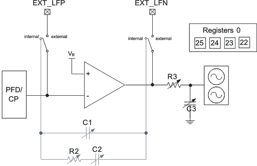 Figure 25. CDCE62002 Loop Filter Topology
9.3.5.8 Internal Loop Filter Component Configuration
Figure 25 illustrates the switching between four fixed internal loop filter settings and the external loop filter setting. Table 12 shows that the CDCE62002 has 16 settings different settings for the loop filter. Four of the settings are internal and twelve are external.
Table 12. CDCE62002 Loop Filter Settings
| LFRCSEL | Charge Pump |
|||||||||
|---|---|---|---|---|---|---|---|---|---|---|
| 3 | 2 | 1 | 0 | Loop Filter | C1 | C2 | R2 | R3 | C3 | Current |
| 0 | 0 | 0 | 0 | Internal | 1.5 pF | 473.5 pF | 4.0k | 5k | 2.5 pF | 1.5 mA |
| 0 | 0 | 0 | 1 | Internal | 1.5 pF | 473.5 pF | 4.0k | 5k | 2.5 pF | 400 μA |
| 0 | 0 | 1 | 0 | Internal | 1.5 pF | 473.5 pF | 2.7k | 5k | 2.5 pF | 250 μA |
| 0 | 0 | 1 | 1 | Internal | 1.5 pF | 473.5 pF | 2.7k | 5k | 2.5 pF | 150 μA |
| 0 | 1 | 0 | 0 | External | X | X | X | 20k | 112 pF | 1.0 mA |
| 0 | 1 | 0 | 1 | External | X | X | X | 20k | 112 pF | 2.0 mA |
| 0 | 1 | 1 | 0 | External | X | X | X | 20k | 112 pF | 3.0 mA |
| 0 | 1 | 1 | 1 | External | X | X | X | 20k | 112 pF | 3.75 mA |
| 1 | 0 | 0 | 0 | External | X | X | X | 10k | 100 pF | 1.0 mA |
| 1 | 0 | 0 | 1 | External | X | X | X | 10k | 100 pF | 2.0 mA |
| 1 | 0 | 1 | 0 | External | X | X | X | 10k | 100 pF | 3.0 mA |
| 1 | 0 | 1 | 1 | External | X | X | X | 10k | 100 pF | 3.75 mA |
| 1 | 1 | 0 | 0 | External | X | X | X | 5k | 100 pF | 1.0 mA |
| 1 | 1 | 0 | 1 | External | X | X | X | 5k | 64 pF | 2.0 mA |
| 1 | 1 | 1 | 0 | External | X | X | X | 5k | 48 pF | 3.0 mA |
| 1 | 1 | 1 | 1 | External | X | X | X | 5k | 38 pF | 3.75 mA |
9.3.6 Lock Detect
The CDCE62002 provides a lock detect indicator circuit that can be detected on an external Pin PLL_LOCK (Pin 32) and internally by reading PLLLOCKPIN bit (6) in Register 2.
Two signals whose phase difference is less than a prescribed amount are locked otherwise they are unlocked. The phase frequency detector / charge pump compares the clock provided by the input divider and the feedback divider; using the input divider as the phase reference. The lock detect circuit implements a programmable lock detect window. Table 13 shows an overview of how to configure the lock detect feature. The PLL_LOCK pin will possibly jitter several times between lock and out of lock until the PLL achieves a stable lock. If desired, choosing a wide loop bandwidth and a high number of successive clock cycles virtually eliminates this characteristic. PLL_LOCK will return to out of lock, if just one cycle is outside the lock detect window or if a cycle slip occurs.
 Figure 26. CDCE62002 Lock Detect
Table 13. CDCE62002 Lock Detect Control
| LOCK DETECT | LOCK DETECT WINDOW | ||
|---|---|---|---|
| BIT NAME → | LOCKW(1) | LOCKW(0) | |
| REGISTER NAME → | 0.13 | 0.14 | |
| 0 | 0 | 2.1 ns | |
| 0 | 1 | 4.6 ns | |
| 1 | 0 | 7.2 ns | |
| 1 | 1 | 19.9 ns | |
9.3.7 Crystal Input Interface
In fundamental mode, TI recommends the oscillation mode of operation for the input crystal and parallel resonance is the recommended type of circuit for the crystal.
A crystal load capacitance refers to all capacitances in the oscillator feedback loop. It is equal to the amount of capacitance seen between the terminals of the crystal in the circuit. For parallel resonant mode circuits, the correct load capacitance is necessary to ensure the oscillation of the crystal within the expected parameters.
The CDCE62002 implements an input crystal oscillator circuitry, known as the Colpitts oscillator, and requires one pad of the crystal to interface with the AUX_IN pin; the other pad of the crystal is tied to ground. In this crystal interface, it is important to account for all sources of capacitance when calculating the correct value for the discrete capacitor component, CL, for a design.
The CDCE62002 has been characterized with 10-pF parallel resonant crystals. The input crystal oscillator stage in the CDCE62002 is designed to oscillate at the correct frequency for all parallel resonant crystals with low-pull capability and rated with a load capacitance that is equal to the sum of the on-chip load capacitance at the AUX_IN pin (10-pF), crystal stray capacitance, and board parasitic capacitance between the crystal and AUX_IN pin.
The normalized frequency error of the crystal, as a result of load capacitance mismatch, can be calculated as Equation 4:

where
- CS is the motional capacitance of the crystal
- C0 is the shunt capacitance of the crystal
- CL,R is the rated load capacitance for the crystal
- CL,A is the actual load capacitance in the implemented PCB for the crystal
- Δf is the frequency error of the crystal
- f is the rated frequency of the crystal
The first three parameters can be obtained from the crystal vendor.
To minimize the frequency error of the crystal to meet application requirements, the difference between the rated load capacitance and the actual load capacitance must be minimized and a crystal with low-pull capability (low CS) must be used.
For example, if an application requires less than ±50-ppm frequency error and a crystal with less than ±50-ppm frequency tolerance is picked, the characteristics are as follows: C0 = 7 pF, CS = 10 pF, and CL,R = 12 pF. To meet the required frequency error, calculate CL,A using Equation 4 to be 17 pF. Subtracting CL,R from CL,A, results in 5 pF; take care during printed-circuit board (PCB) layout with the crystal and the CDCE62002 to ensure that the sum of the crystal stray capacitance and board parasitic capacitance is less than the calculated 5 pF.
Good layout practices are fundamental to the correct operation and reliability of the oscillator. It is critical to place the crystal components very close to the XIN pin to minimize routing distances. Long traces in the oscillator circuit are a very common source of problems. Do not route other signals across the oscillator circuit. Also, make sure power and high-frequency traces are routed as far away as possible to avoid crosstalk and noise coupling. Avoid the use of vias; if the routing becomes very complex, it is better to use 0-Ω resistors as bridges to go over other signals. Vias in the oscillator circuit must only be used for connections to the ground plane. Do not share ground connections; instead, make a separate connection to ground for each component that requires grounding. If possible, place multiple vias in parallel for each connection to the ground plane. Especially in the Colpitts oscillator configuration, the oscillator is very sensitive to capacitance in parallel with the crystal. Therefore, the layout must be designed to minimize stray capacitance across the crystal to less than 5 pF total under all circumstances to ensure proper crystal oscillation. Be sure to take into account both PCB and crystal stray capacitance.
9.3.8 VCO Calibration
The CDCE62002 includes two on-chip LC oscillator-based VCOs with low phase noise covering a frequency range of 1.75 GHz to 2.356 GHz. The VCO must be calibrated to ensure proper operation over the valid device operating conditions. VCO calibration is controlled by the reference clock input. This calibration requires that the PLL be set up properly to lock the PLL loop and that the reference clock input be present.
The device enters self-calibration of the VCO automatically at power up, after the registers have been loaded from the EEPROM and an input clock signal is detected. If there is no input clock available during power up, the VCO will wait for reference clock before starting calibration.
If the input signal is not valid during self-calibration, it is necessary to re-initiate VCO calibration after the input clock signal stabilizes.
NOTE
Re-calibration is also necessary anytime a PLL setting is changed (e.g. divider ratios in the PLL or loop filter settings are adjusted).
VCO calibration can be initiated by writing to register 2 bits 7, 13 and 20.
Table 14. VCO Calibration Method Through Register Programming
| CALSELECT Reg 2.13 |
PLLRESET 2.20 |
PD 2.7 |
VCO CALIBRATION MECHANISM(1) |
|---|---|---|---|
| 1 | 1-0-1 | 1 | VCO calibration starts at PLLRESET toggling low-to-high. The outputs turn off for the duration of the calibration, which is a few ns. |
| 0 | X | 1-0-1 | Device is powered down when PD is toggle 1-to-0. All outputs are disabled while PD is zero. After asserting PD from zero to one the VCO becomes calibrated and immediately afterwards the device outputs turn on. |
9.3.9 Start-Up Time Estimation
The CDCE62002 startup time can be estimated based on the parameters defined in Table 15 and graphically shown in Figure 27.
Table 15. Start-up Time Dependencies
| PARAMETER | DESCRIPTION | METHOD OF DETERMINATION | |
|---|---|---|---|
| tpul | Power-up time (low limit) | Power-supply rise time to low limit of power-on-reset (POR) trip point | Time required for power supply to ramp to 2.27 V |
| tpuh | Power-up time (high limit) | Power-supply rise time to high limit of power-on-reset (POR) trip point | Time required for power supply to ramp to 2.64 V |
| trsu | Reference start-up time | After POR releases, the Colpitts oscillator is enabled. This start-up time is required for the oscillator to generate the requisite signal levels for the delay block to be clocked by the reference input | 500 µs best-case and 800 µs worst-case (This is only for crystal connected to AUX_IN) |
| tdelay | Delay time | Internal delay time generated from the clock. This delay provides time for the oscillator to stabilize. | tdelay = 16384 x tid
tid = period of input clock to the input divider |
| tVCO_CAL | VCO calibration time | VCO calibration time generated from the PFD clock. This process selects the operating point for the VCO based on the PLL settings. | tVCO_CAL = 550 x tPFD
tPFD = period of the PFD clock |
| tPLL_LOCK | PLL lock time | Time required for PLL to lock within ±10 ppm of reference frequency | tPLL_LOCK = 3/LBW LBW = PLL Loop Bandwidth |
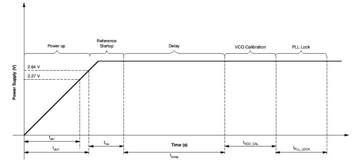 Figure 27. Start-Up Time dependencies
9.4 Device Functional Modes
9.4.1 Clock Generator
The CDCE62002 can generate 1 to 4 low noise clocks from a single crystal or crystal oscillator as follows:
 Figure 28. CDCE62002 as a Clock Generator
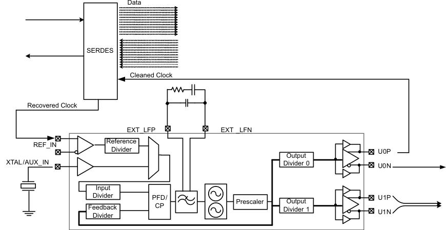
9.4.2 SERDES Start-Up and Clock Cleaner
The CDCE62002 can serve as a SERDES device companion by providing a crystal based reference for the SERDES device to lock to receive data stream and when the SERDES locks to the data and outputs the recovered clock the CDCE62002 can switch and use the recovered clock and serve as a jitter cleaner.
Because the jitter of the recovered clock can be above 100 ps (RMS), the output jitter from CDCE62002 can be as low and 6 ps (RMS) depending on the external loop filter configuration.
9.4.3 Clocking ADCS With the CDCE62002
High-speed analog to digital converters incorporate high input bandwidth on both the analog port and the sample clock port. Often the input bandwidth far exceeds the sample rate of the converter. Engineers regularly implement receiver chains that take advantage of the characteristics of bandpass sampling. This implementation trend often causes engineers working in communications system design to encounter the term clock-limited performance. Therefore, it is important to understand the impact of clock jitter on ADC performance. Equation 5 shows the relationship of data converter signal to noise ratio (SNR) to total jitter:

Total jitter comprises two components: the intrinsic aperture jitter of the converter and the jitter of the sample clock:

With respect to an ADC with N-bits of resolution, ignoring total jitter, ADC quantization error, and input noise, Equation 7 shows the relationship between resolution and SNR:

Figure 30 plots Equation 5 and Equation 7 for constant values of total jitter. When used in conjunction with most ADCs, the CDCE62002 supports a total jitter performance value of <1 ps.
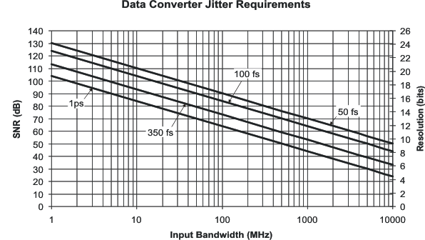 Figure 30. Data Converter Jitter Requirements
9.5 Programming
9.5.1 Interface and Control Block
The interface and control block includes a SPI interface, one control pin, a non-volatile memory array in which the device stores default configuration data, and an array of device registers implemented in static RAM. This RAM, also called the device registers, configures all hardware within the CDCE62002.
9.5.1.1 SPI (Serial Peripheral Interface)
The serial interface of CDCE62002 is a simple bidirectional SPI interface for writing and reading to and from the device registers. It implements a low speed serial communications link in a master/slave topology in which the CDCE62002 is a slave. The SPI consists of four signals:
- SPI_CLK:Serial Clock (Output from Master) – the CDCE62002 and the master host clock data in and out on the rising edge of SPI_CLK. Data transitions therefore occur on the falling edge of the clock. (LVCMOS Input Buffer)
- SPI_MOSI: Master Output Slave Input (LVCMOS Input Buffer).
- SPI_MISO: Master Input Slave Output (Open Drain LVCMOS Buffer)
- SPI_LE: Latch Enable (Output from Master). The falling edge of SPI_LE initiates a transfer. If SPI_LE is high, no data transfer can take place. (LVCMOS Input Buffer).
9.5.1.2 SPI Interface Master
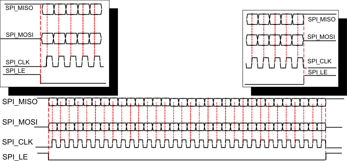
The Interface master can be designed using a FPGA or a microcontroller. The CDCE62002 acts as a slave to the SPI master and only supports non-consecutive read and write command. The SPI clock should start and stop with respect to the SPI_LE signal as shown in Figure 31 SPI_MOSI, SPI_CLK and SPI_LE are generated by the SPI Master. SPI_MISO is generated by the SPI slave the CDCE62002.
9.5.1.3 SPI Consecutive Read/Write Cycles to the CDCE62002
Figure 32 Illustrates how two consecutive SPI cycles are performed between a SPI Master and the CDCE62002 SPI Slave.
 Figure 32. Consecutive Read/Write Cycles
9.5.1.4 Writing to the CDCE62002
Figure 33 illustrates a Write to RAM operation. Notice that the latching of the first data bit in the data stream (Bit 0) occurs on the first rising edge of SPI_CLK after SPI_LE transitions from a high to a low. For the CDCE62002, data transitions occur on the falling edge of SPI_CLK. A rising edge on SPI_LE signals to the CDCE62002 that the transmission of the last bit in the stream (Bit 31) has occurred.
 Figure 33. CDCE62002 SPI Write Operation
9.5.1.5 Reading from the CDCE62002
Figure 34 shows how the CDCE62002 executes a read command. The SPI master first issues a read command to initiate a data transfer from the CDCE62002 back to the host (see SPI Bus Timing Characteristics). This command specifies the address of the register of interest. By transitioning SPI_LE from a low to a high, the CDCE62002 resolves the address specified in the appropriate bits of the data field. The host drives SPI_LE low and the CDCE62002 presents the data present in the register specified in the read command on SPI_MISO.
 Figure 34. CDCE62002 SPI Read Operation
9.5.1.6 Writing to EEPROM
After the CDCE62002 detects a power-up and completes a reset cycle, the device copies the contents of the on-chip EEPROM into the device registers. (SPI_LE signal has to be HIGH in order for the EEPROM to load correctly during the rising edge of power_down signal).
The host issues a special commands shown in Figure 35 to copy the contents of device registers 0 and 1into EERPOM.
- Copy RAM to EEPROM – unlock, execution of this command can happen many times.
After the command is initiated, power must remain stable and the host must not access the CDCE62002 for at least 50 ms to allow the EEPROM to complete the write cycle and to avoid the possibility of EEPROM corruption.
9.5.1.7 CDCE62002 SPI Command Structure
The CDCE62002 supports three commands issued by the master through the SPI:
- Write to RAM
- Read Command
- Copy RAM to EEPROM – unlock
Figure 35 provides a summary of the CDCE62002 SPI command structure. The host (master) constructs a Write to RAM command by specifying the appropriate register address in the address field and appends this value to the beginning of the data field. Therefore, a valid command stream must include 32 bits, transmitted LSB first. The host must issue a read command to initiate a data transfer from the CDCE62002 back to the host. This command specifies the address of the register of interest in the data field.

NOTE:
‘A’ indicates address bits.9.5.2 Device Configuration
The Feature Description section described four different functional blocks contained within the CDCE62002. Figure 36 depicts these blocks along with a high-level functional block diagram of the circuit elements comprising each block. The balance of this section focuses on a detailed discussion of each functional block from the perspective of how to configure them.
9.6 Register Maps
9.6.1 Device Registers: Register 0 Address 0x00
Table 16. CDCE62002 Register 0 Bit Definitions
| REGISTER BIT |
BIT NAME |
RELATED BLOCK | DESCRIPTION / FUNCTION | |
|---|---|---|---|---|
| 0 | INBUFSELX | INBUFSELX | Input Buffer Select (LVPECL,LVDS or LVCMOS) XY(00 ) Disabled, (01) LVDS, (10) LVPECL, (11) LVCMOS The VBB internal Biasing will be determined from this setting |
EEPROM |
| 1 | INBUFSELY | INBUFSELY | EEPROM | |
| 2 | REFSEL | Smart MUX Bits(2,3) |
See specific section for more detailed description and configuration setup.
00 – RESERVED 10 – REF_IN Select 01– AUX_IN Select 11 – Auto Select ( Reference then AUX) |
EEPROM |
| 3 | AUXSEL | EEPROM | ||
| 4 | ACDCSEL | Input Buffers | If Set to 1 DC Termination, If set to “0” AC Termination | EEPROM |
| 5 | TERMSEL | Input Buffers | If Set to 0 Input Buffer Internal Termination Enabled | EEPROM |
| 6 | REFDIVIDE 0 | Reference Divider Settings (Refer to Table 5) See specific section for more detailed description and configuration setup. |
EEPROM | |
| 7 | REFDIVIDE 1 | EEPROM | ||
| 8 | REFDIVIDE 2 | EEPROM | ||
| 9 | REFDIVIDE 3 | EEPROM | ||
| 10 | RESERVED | Always Set to 0 | EEPROM | |
| 11 | I70TEST | TEST | Set to 0 for Normal Operation. | EEPROM |
| 12 | ATETEST | TEST | Set to 0 for Normal Operation. | EEPROM |
| 13 | LOCKW(0) | PLL Lock | Lock-detect window Bit 0 | EEPROM |
| 14 | LOCKW(1) | PLL Lock | Lock-detect window Bit 1 | EEPROM |
| 15 | OUT0DIVRSEL0 | Output 0 | Output 0 Divider Settings (Refer to Table 6) See specific section for more detailed description and configuration setup. |
EEPROM |
| 16 | OUT0DIVRSEL1 | Output 0 | EEPROM | |
| 17 | OUT0DIVRSEL2 | Output 0 | EEPROM | |
| 18 | OUT0DIVRSEL3 | Output 0 | EEPROM | |
| 19 | OUT1DIVRSEL0 | Output 1 | Output 1 Divider Settings (Refer to Table 6) See specific section for more detailed description and configuration setup. |
EEPROM |
| 20 | OUT1DIVRSEL1 | Output 1 | EEPROM | |
| 21 | OUT1DIVRSEL2 | Output 1 | EEPROM | |
| 22 | OUT1DIVRSEL3 | Output 1 | EEPROM | |
| 23 | HIPERORMANCE | Output 0 & 1 | High Performance, If this Bit is set to 1: – Increases the Bias in the device to achieve Best Phase Noise on the Output Divider – It changes the LVPECL Buffer to Hi Swing in LVPECL. – It increases the current consumption by 20mA (Typical) – This setting only applies to LVPECL output buffers. If none of these two outputs are LVPECL, this bit should be set to zero. |
EEPROM |
| 24 | OUTBUFSEL0X | Output 0 | Output Buffer mode select for OUTPUT 0 . (X,Y)=00:Disabled, 01:LVCMOS, 10:LVDS, 11:LVPECL |
EEPROM |
| 25 | OUTBUFSEL0Y | Output 0 | EEPROM | |
| 26 | OUTBUFSEL1X | Output 1 | Output Buffer mode select for OUTPUT 1 . (X,Y)=00:Disabled, 01:LVCMOS, 10:LVDS, 11:LVPECL |
EEPROM |
| 27 | OUTBUFSEL1Y | Output 1 | EEPROM |
Table 17. Reference Input AC/DC Input Termination Table
9.6.2 Device Registers: Register 1 Address 0x01
Table 18. CDCE62002 Register 1 Bit Definitions
| REGISTER BIT |
BIT NAME | RELATED BLOCK |
DESCRIPTION / FUNCTION | |
|---|---|---|---|---|
| 0 | SELVCO | VCO Core | VCO Select – See Table 10 for details | EEPROM |
| 1 | SELINDIV0 | VCO Core | Input Divider Settings (Refer to Table 7) See specific section for more detailed description and configuration setup. |
EEPROM |
| 2 | SELINDIV1 | VCO Core | EEPROM | |
| 3 | SELINDIV2 | VCO Core | EEPROM | |
| 4 | SELINDIV3 | VCO Core | EEPROM | |
| 5 | SELINDIV4 | VCO Core | EEPROM | |
| 6 | SELINDIV5 | VCO Core | EEPROM | |
| 7 | SELINDIV6 | VCO Core | EEPROM | |
| 8 | SELINDIV7 | VCO Core | EEPROM | |
| 9 | SELPRESCA | VCO Core | PRESCALER Setting. (Refer to Table 11) See specific section for more detailed description and configuration setup. |
EEPROM |
| 10 | SELPRESCB | VCO Core | EEPROM | |
| 11 | SELFBDIV0 | VCO Core | FEEDBACK DIVIDER Setting (Refer to Table 8) See specific section for more detailed description and configuration setup. |
EEPROM |
| 12 | SELFBDIV1 | VCO Core | EEPROM | |
| 13 | SELFBDIV2 | VCO Core | EEPROM | |
| 14 | SELFBDIV3 | VCO Core | EEPROM | |
| 15 | SELFBDIV4 | VCO Core | EEPROM | |
| 16 | SELFBDIV5 | VCO Core | EEPROM | |
| 17 | SELFBDIV6 | VCO Core | EEPROM | |
| 18 | SELFBDIV7 | VCO Core | EEPROM | |
| 19 | SELBPDIV0 | VCO Core | BYPASS DIVIDER Setting (Refer to Table 9) See specific section for more detailed description and configuration setup. | EEPROM |
| 20 | SELBPDIV1 | VCO Core | EEPROM | |
| 21 | SELBPDIV2 | VCO Core | EEPROM | |
| 22 | LFRCSEL0 | VCO Core | Loop Filter & Charge Pump Control Setting (Refer to Table 12) See specific section for more detailed description and configuration setup. |
EEPROM |
| 23 | LFRCSEL1 | VCO Core | EEPROM | |
| 24 | LFRCSEL2 | VCO Core | EEPROM | |
| 25 | LFRCSEL3 | VCO Core | EEPROM | |
| 26 | RESERVED | Status | TI Use Only; set 0 | EEPROM |
| 27 | RESERVED | Status | Read Only; May read back to 1 or 0; set '1' while writing | EEPROM |

