ZHCSGW5B January 2017 – October 2020 CC2640R2F-Q1
PRODUCTION DATA
- 1 特性
- 2 应用
- 3 说明
- 4 功能方框图
- 5 Revision History
- 6 Device Comparison
- 7 Terminal Configuration and Functions
-
8 Specifications
- 8.1 Absolute Maximum Ratings
- 8.2 ESD Ratings
- 8.3 Recommended Operating Conditions
- 8.4 Power Consumption Summary
- 8.5 General Characteristics
- 8.6 1-Mbps GFSK (Bluetooth low energy Technology) – RX
- 8.7 1-Mbps GFSK (Bluetooth low energy Technology) – TX
- 8.8 24-MHz Crystal Oscillator (XOSC_HF)
- 8.9 32.768-kHz Crystal Oscillator (XOSC_LF)
- 8.10 48-MHz RC Oscillator (RCOSC_HF)
- 8.11 32-kHz RC Oscillator (RCOSC_LF)
- 8.12 ADC Characteristics
- 8.13 Temperature Sensor
- 8.14 Battery Monitor
- 8.15 Continuous Time Comparator
- 8.16 Low-Power Clocked Comparator
- 8.17 Programmable Current Source
- 8.18 Synchronous Serial Interface (SSI)
- 8.19 DC Characteristics
- 8.20 Thermal Resistance Characteristics for RGZ Package
- 8.21 Timing Requirements
- 8.22 Switching Characteristics
- 8.23 Typical Characteristics
- 9 Detailed Description
- 10Application, Implementation, and Layout
- 11Device and Documentation Support
- 12Mechanical, Packaging, and Orderable Information
11.1 Device Nomenclature
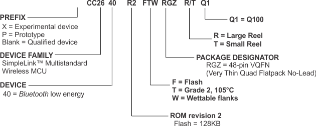
To designate the stages in the product development cycle, TI assigns prefixes to all part numbers and date-code. Each device has one of three prefixes/identifications: X, P, or null (no prefix) (for example, CC2640R2F-Q1 is in production; therefore, no prefix/identification is assigned).
Device development evolutionary flow:
- XExperimental device that is not necessarily representative of the final device's electrical specifications and may not use production assembly flow.
- PPrototype device that is not necessarily the final silicon die and may not necessarily meet final electrical specifications.
- nullProduction version of the silicon die that is fully qualified.
Production devices have been characterized fully, and the quality and reliability of the device have been demonstrated fully. TI's standard warranty applies.
Predictions show that prototype devices (X or P) have a greater failure rate than the standard production devices. Texas Instruments recommends that these devices not be used in any production system because their expected end-use failure rate still is undefined. Only qualified production devices are to be used.
TI device nomenclature also includes a suffix with the device family name. This suffix indicates the package type (for example, RGZ).
For orderable part numbers of the CC2640R2F-Q1 device package types, see the Package Option Addendum of this document, the TI website (www.ti.com), or contact your TI sales representative.
 Figure 11-1 Device Nomenclature