ZHCSCF9 May 2014 BUF16821-Q1
PRODUCTION DATA.
- 1 特性
- 2 应用范围
- 3 说明
- 4 修订历史记录
- 5 Pin Configuration and Functions
- 6 Specifications
-
7 Detailed Description
- 7.1 Overview
- 7.2 Functional Block Diagram
- 7.3 Feature Description
- 7.4 Device Functional Modes
- 7.5 Programming
- 7.6 Register Maps
- 8 Application and Implementation
- 9 Power Supply Recommendations
- 10Layout
- 11器件和文档支持
- 12机械封装和可订购信息
6 Specifications
6.1 Absolute Maximum Ratings
over operating free-air temperature range (unless otherwise noted)(1)| MIN | MAX | UNIT | |||
|---|---|---|---|---|---|
| VS | Supply voltage | 22 | V | ||
| DVDD | Digital power supply (VSD pin) | 6 | V | ||
| Digital input pins | SCL, SDA, AO, BKSEL: voltage | –0.5 | 6 | V | |
| SCL, SDA, AO, BKSEL: current | ±10 | mA | |||
| Output pins, OUT1 through OUT16, VCOM1 and VCOM2(2) | (V–) – 0.5 | (V+) + 0.5 | V | ||
| Output short-circuit(3) | Continuous | ||||
| Ambient operating temperature | –40 | 95 | °C | ||
| TJ | Junction temperature | 125 | °C | ||
(1) Stresses beyond those listed under Absolute Maximum Ratings may cause permanent damage to the device. These are stress ratings only, which do not imply functional operation of the device at these or any other conditions beyond those indicated under Recommended Operating Conditions. Exposure to absolute-maximum-rated conditions for extended periods may affect device reliability.
(2) See the Output Protection section.
(3) Short-circuit to ground, one amplifier per package.
6.2 Handling Ratings
| MIN | MAX | UNIT | ||||
|---|---|---|---|---|---|---|
| Tstg | Storage temperature range | –65 | 150 | °C | ||
| V(ESD) | Electrostatic discharge | Human body model (HBM), per AEC Q100-002(1) | –2000 | 2000 | V | |
| Charged device model (CDM), per AEC Q100-011 | Corner pins (1, 14, 15, and 28) | –750 | 750 | |||
| Other pins | –500 | 500 | ||||
(1) AEC Q100-002 indicates HBM stressing is done in accordance with the ANSI/ESDA/JEDEC JS-001 specification.
6.3 Recommended Operating Conditions
over operating free-air temperature range (unless otherwise noted)| MIN | NOM | MAX | UNIT | ||
|---|---|---|---|---|---|
| VS | Supply voltage | 9.0 | 18.0 | 20.0 | V |
| DVDD | Digital power supply (VSD pin) | 2.0 | 3.3 | 5.5 | V |
6.4 Thermal Information
| THERMAL METRIC(1) | BUF16821-Q1 | UNIT | |
|---|---|---|---|
| PWP (HTSSOP) | |||
| 28 PINS | |||
| RθJA | Junction-to-ambient thermal resistance | 34.3 | °C/W |
| RθJC(top) | Junction-to-case (top) thermal resistance | 19.9 | |
| RθJB | Junction-to-board thermal resistance | 17.4 | |
| ψJT | Junction-to-top characterization parameter | 0.7 | |
| ψJB | Junction-to-board characterization parameter | 17.2 | |
| RθJC(bot) | Junction-to-case (bottom) thermal resistance | 3.0 | |
(1) For more information about traditional and new thermal metrics, see the IC Package Thermal Metrics application report, SPRA953.
6.5 Electrical Characteristics
At TA = 25°C, VS = 18 V, VSD = 2 V, RL = 1.5 kΩ connected to ground, and CL = 200 pF, unless otherwise noted.| PARAMETER | CONDITIONS | MIN | TYP | MAX | UNIT | ||
|---|---|---|---|---|---|---|---|
| ANALOG GAMMA BUFFER CHANNELS | |||||||
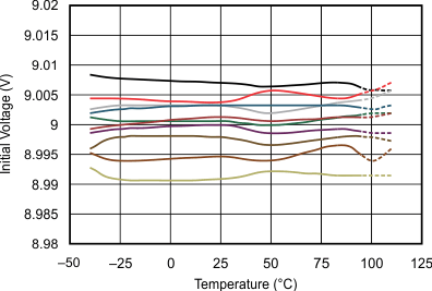
| Reset value | Code 512 | 9 | V | ||||
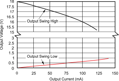
| OUT 1–16 output swing: high | Code = 1023, sourcing 10 mA, TA = –40°C to 85°C | 17.7 | 17.85 | V | |||
| OUT 1–16 output swing: low | Code = 0, sinking 10 mA, TA = –40°C to 85°C | 0.07 | 0.3 | V | |||
| VCOM1, 2 output swing: high | Code = 1023, sourcing 100 mA, TA = –40°C to 85°C | 13 | 16.2 | V | |||
| VCOM1, 2 output swing: low | Code = 0, sinking 100 mA, TA = –40°C to 85°C | 0.6 | 2 | V | |||
| Continuous output current(1) | 30 | mA | |||||
| Output accuracy | ±20 | ±50 | mV | ||||
| Output accuracy over temperature | Code 512, TA = –40°C to 85°C | ±25 | μV/°C | ||||
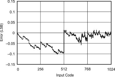
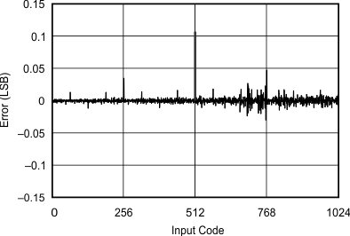
| INL | Integral nonlinearity | 0.3 | LSB | ||||
| DNL | Differential nonlinearity | 0.3 | LSB | ||||
| ΔVO(ΔIO) | Load regulation, 10 mA | Code 512 or VCC / 2, IOUT = 5-mA to –5-mA step | 0.5 | 1.5 | mV/mA | ||
| OTP MEMORY | |||||||
| Number of OTP write cycles | 16 | Cycles | |||||
| Memory retention | 100 | Years | |||||
| ANALOG POWER SUPPLY | |||||||
| Operating range | 9 | 20 | V | ||||
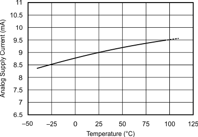
| ICC(tot) | Total analog supply current | Outputs at reset values, no load | 12 | 14 | mA | ||
| ICC(tot) over temperature | TA = –40°C to 85°C | 18 | mA | ||||
| DIGITAL | |||||||
| VIH | Logic 1 high input voltage | 0.7 × VSD | V | ||||
| VIL | Logic 0 low input voltage | 0.3 × VSD | V | ||||
| VOL | Logic 0 low output voltage | ISINK = 3 mA | 0.15 | 0.4 | V | ||
| Input leakage | ±0.01 | ±10 | μA | ||||
| fCLK | Clock frequency | Standard, fast mode, TA = –40°C to 85°C | 400 | kHz | |||
| High-speed mode, TA = –40°C to 85°C | 2.7 | MHz | |||||
| DIGITAL POWER SUPPLY | |||||||
| DVDD | Digital power supply (VSD pin) | 2.0 | 5.5 | V | |||
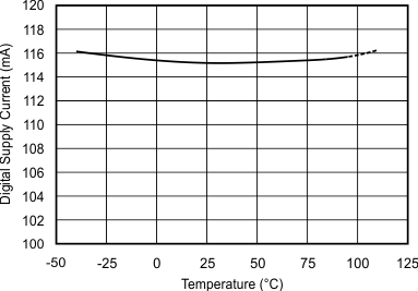
| ISD | Digital supply current(1) | Outputs at reset values, no load, two-wire bus inactive | 115 | 150 | μA | ||
| ISD over temperature | TA = –40°C to 85°C | 115 | μA | ||||
| TEMPERATURE RANGE | |||||||
| Specified range | –40 | 85 | °C | ||||
| Operating range | Junction temperature < 125°C | –40 | 95 | °C | |||
| Storage range | –65 | 150 | °C | ||||
| RθJA | Thermal resistance, HTSSOP-28(1)(2) |
40 | °C/W | ||||
(1) Observe maximum power dissipation.
(2) Thermal pad is attached to the printed circuit board (PCB), 0-lfm airflow, and 76-mm × 76-mm copper area.
6.6 Timing Requirements
| PARAMETER | FAST MODE | HIGH-SPEED MODE | UNIT | |||
|---|---|---|---|---|---|---|
| MIN | MAX | MIN | MAX | |||
| f(SCL) | SCL operating frequency | 0.001 | 0.4 | 0.001 | 2.7 | MHz |
| t(BUF) | Bus free time between stop and start conditions | 1300 | 230 | ns | ||
| t(HDSTA) | Hold time after repeated start condition. After this period, the first clock is generated. | 600 | 230 | ns | ||
| t(SUSTA) | Repeated start condition setup time | 600 | 230 | ns | ||
| t(SUSTO) | Stop condition setup time | 600 | 230 | ns | ||
| t(HDDAT) | Data hold time | 20 | 900 | 20 | 130 | ns |
| t(SUDAT) | Data setup time | 100 | 20 | ns | ||
| t(LOW) | SCL clock low period | 1300 | 230 | ns | ||
| t(HIGH) | SCL clock high period | 600 | 60 | ns | ||
| tR(SDA), tF(SDA) | Data rise and fall time | 300 | 80 | ns | ||
| tR(SCL), tF(SCL) | Clock rise and fall time | 300 | 40 | ns | ||
| tR | Clock and data rise time for SCLK ≤ 100 kHz | 1000 | ns | |||
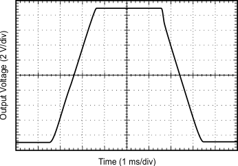
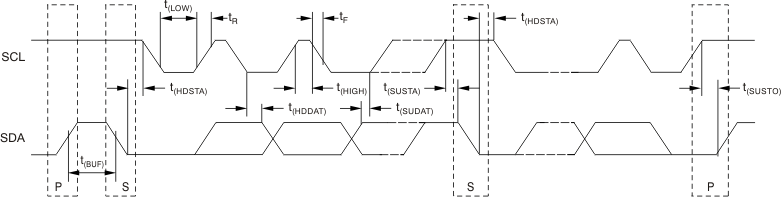 Figure 1. Timing Requirements Diagram
6.7 Typical Characteristics
At TA = 25°C, VS = 18 V, VSD = 2 V, RL = 1.5 kΩ connected to ground, and CL = 200 pF, unless otherwise noted.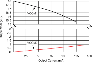
(VCOM1 and VCOM2)
| 10 Typical Units Shown | ||
(Channels 1–16)