ZHCSCI8 May 2014
PRODUCTION DATA.
- 1 特性
- 2 应用范围
- 3 说明
- 4 简化电路原理图
- 5 修订历史记录
- 6 Pin Configuration and Functions
- 7 Specifications
-
8 Detailed Description
- 8.1 Overview
- 8.2 Functional Block Diagram
- 8.3 Feature Description
- 8.4 Device Functional Modes
- 8.5 Register Maps
-
9 Applications and Implementation
- 9.1 Application Information
- 9.2
Typical Applications
- 9.2.1
WPC Power Supply 5-V Output With 1-A Maximum Current and I2C
- 9.2.1.1 Design Requirements
- 9.2.1.2
Detailed Design Procedure
- 9.2.1.2.1 Output Voltage Set Point
- 9.2.1.2.2 Output and Rectifier Capacitors
- 9.2.1.2.3 Maximum Output Current Set Point
- 9.2.1.2.4 TERM Pin
- 9.2.1.2.5 I2C
- 9.2.1.2.6 Communication Current Limit
- 9.2.1.2.7 Receiver Coil
- 9.2.1.2.8 Series and Parallel Resonant Capacitors
- 9.2.1.2.9 Communication, Boot, and Clamp Capacitors
- 9.2.1.3 Application Performance Plots
- 9.2.2 bq5102x Standalone in System Board or Back Cover
- 9.2.1
WPC Power Supply 5-V Output With 1-A Maximum Current and I2C
- 10Power Supply Recommendations
- 11Layout
- 12器件和文档支持
- 13机械封装和可订购信息
7 Specifications
7.1 Absolute Maximum Ratings
over operating free-air temperature range (unless otherwise noted)(1)(2)| PIN | MIN | MAX | UNIT | |
|---|---|---|---|---|
| Input voltage | AC1, AC2 | –0.8 | 20 | V |
| RECT, COMM1, COMM2, OUT, , CLAMP1, CLAMP2, WPG, PD_DET | –0.3 | 20 | ||
| AD, AD-EN | –0.3 | 30 | ||
| BOOT1, BOOT2 | –0.3 | 20 | ||
| SCL, SDA, TERM, CM_ILIM, FOD, TS/CTRL, ILIM, TMEM, VTSB, VO_REG, LPRBEN | –0.3 | 7 | ||
| Input current | AC1, AC2 (RMS) | 2.5 | A | |
| Output current | OUT | 1.5 | A | |
| Output sink current | WPG, PD_DET | 15 | mA | |
| Output sink current | COMM1, COMM2 | 1.0 | A | |
| TJ, junction temperature | –40 | 150 | °C |
(1) All voltages are with respect to the PGND pin, unless otherwise noted.
(2) Stresses beyond those listed under absolute maximum ratings may cause permanent damage to the device. These are stress ratings only, and functional operation of the device at these or any other conditions beyond those indicated under recommended operating conditions is not implied. Exposure to absolute-maximum-rated conditions for extended periods may affect device reliability.
7.2 Handling Ratings
| MIN | MAX | UNIT | |||
|---|---|---|---|---|---|
| Tstg | Storage temperature range | –65 | 150 | °C | |
| VESD(1) | Electrostatic discharge | Human body model (HBM), per ANSI/ESDA/JEDEC JS-001, all pins(2), 100 pF, 1.5 kΩ | –2 | 2 | kV |
| Charged device model (CDM), per JEDEC specification JESD22-C101, all pins(3) | –500 | 500 | V | ||
(1) Electrostatic discharge (ESD) to measure device sensitivity and immunity to damage caused by assembly line electrostatic discharges in to the device.
(2) JEDEC document JEP155 states that 500-V HBM allows safe manufacturing with a standard ESD control process.
(3) JEDEC document JEP157 states that 250-V CDM allows safe manufacturing with a standard ESD control process.
7.3 Recommended Operating Conditions
over operating free-air temperature range (unless otherwise noted)| MIN | MAX | UNIT | ||
|---|---|---|---|---|
| VRECT | RECT voltage | 4.0 | 10.0 | V |
| IOUT | Output current | 1.0 | A | |
| IAD-EN | Sink current | 1 | mA | |
| ICOMM | COMMx sink current | 500 | mA | |
| TJ | Junction temperature | 0 | 125 | ºC |
7.4 Thermal Information
| THERMAL METRIC(1) | bq5102x | UNIT | |
|---|---|---|---|
| YFP (42 PINS) | |||
| RθJA | Junction-to-ambient thermal resistance(2) | 49.7 | °C/W |
| RθJC(top) | Junction-to-case (top) thermal resistance(3) | 0.2 | |
| RθJB | Junction-to-board thermal resistance(4) | 6.1 | |
| ψJT | Junction-to-top characterization parameter(5) | 1.4 | |
| ψJB | Junction-to-board characterization parameter(6) | 6.0 | |
(1) For more information about traditional and new thermal metrics, see the IC Package Thermal Metrics application report, SPRA953.
(2) The junction-to-ambient thermal resistance under natural convection is obtained in a simulation on a JEDEC-standard, high-K board, as specified in JESD51-7, in an environment described in JESD51-2a.
(3) The junction-to-case (top) thermal resistance is obtained by simulating a cold plate test on the package top. No specific JEDEC-standard test exists, but a close description can be found in the ANSI SEMI standard G30-88.
(4) The junction-to-board thermal resistance is obtained by simulating in an environment with a ring cold plate fixture to control the PCB temperature, as described in JESD51-8.
(5) The junction-to-top characterization parameter, ψJT, estimates the junction temperature of a device in a real system and is extracted from the simulation data for obtaining RθJA, using a procedure described in JESD51-2a (sections 6 and 7).
(6) The junction-to-board characterization parameter, ψJB, estimates the junction temperature of a device in a real system and is extracted from the simulation data for obtaining RθJA , using a procedure described in JESD51-2a (sections 6 and 7).
7.5 Electrical Characteristics
over operating free-air temperature range (unless otherwise noted) , ILOAD = IOUT| PARAMETER | TEST CONDITIONS | MIN | TYP | MAX | UNIT | |
|---|---|---|---|---|---|---|
| VUVLO | Undervoltage lockout | VRECT: 0 to 3 V | 2.8 | 2.9 | V | |
| VHYS-UVLO | Hysteresis on UVLO | VRECT: 3 to 2 V | 393 | mV | ||
| VRECT-OVP | Input overvoltage threshold | VRECT: 5 to 16 V | 14.6 | 15.1 | 15.6 | V |
| VHYS-OVP | Hysteresis on OVP | VRECT: 16 to 5 V | 1.5 | V | ||
| VRECT(REG) | Voltage at RECT pin set by communication with primary | VOUT + 0.120 | VOUT + 2.0 | V | ||
| VRECT(TRACK) | VRECT regulation above VOUT | VILIM = 1.2 V | 140 | mV | ||
| ILOAD-HYS | ILOAD hysteresis for dynamic VRECT thresholds as a % of IILIM | ILOAD falling | 4 | |||
| VRECT-DPM | Rectifier under voltage protection, restricts IOUT at VRECT-DPM | 3 | 3.1 | 3.2 | V | |
| VRECT-REV | Rectifier reverse voltage protection with a supply at the output | VRECT-REV = VOUT – VRECT, VOUT = 10 V | 8.8 | 9.2 | V | |
| QUIESCENT CURRENT | ||||||
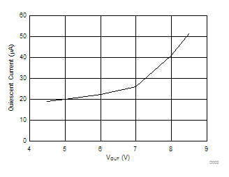
| IOUT(standby) | Quiescent current at the output when wireless power is disabled | VOUT ≤ 5 V, 0°C ≤ TJ ≤ 85°C | 20 | 35 | µA | |
| ILIM SHORT CIRCUIT | ||||||
| RILIM-SHORT | Highest value of RILIM resistor considered a fault (short). Monitored for IOUT > 100 mA | RILIM: 200 to 50 Ω. IOUT latches off, cycle power to reset | 209 | 235 | Ω | |
| tDGL-Short | Deglitch time transition from ILIM short to IOUT disable | 1 | ms | |||
| ILIM_SC | ILIM-SHORT,OK enables the ILIM short comparator when IOUT is greater than this value | ILOAD: 0 to 200 mA | 110 | 125 | 140 | mA |
| ILIM-SHORT,OK HYSTERESIS | Hysteresis for ILIM-SHORT,OK comparator | ILOAD: 200 to 0 mA | 20 | mA | ||
| IOUT-CL | Maximum output current limit | Maximum ILOAD that can be delivered for 1 ms when ILIM is shorted | 3.7 | A | ||
| OUTPUT | ||||||
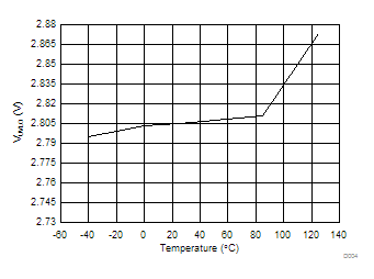
| VO_REG | Feedback voltage set point | ILOAD = 1000 mA | 0.4950 | 0.5013 | 0.5075 | V |
| ILOAD = 1 mA | 0.4951 | 0.5014 | 0.5076 | |||
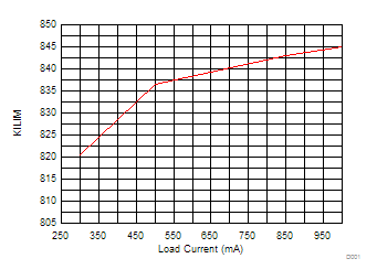
| KILIM | Current programming factor for hardware short circuit protection | RILIM = KILIM / IILIM, where IILIM is the hardware current limit IOUT = 850 mA |
842 | AΩ | ||
| IOUT_RANGE | Current limit programming range | 1500 | mA | |||
| ICOMM | Output current limit during communication | IOUT ≥ 320 mA | IOUT – 50 | mA | ||
| 100 mA ≤ IOUT < 320 mA | IOUT + 50 | |||||
| IOUT < 100 mA | 200 | |||||
| tHOLD-OFF | Hold off time for the communication current limit during startup | 1 | s | |||
| TS/CTRL | ||||||
| VTS-Bias | TS bias voltage (internal) | ITS-Bias < 100 µA and communication is active (periodically driven, see tTS/CTRL-Meas) | 1.8 | V | ||
| VCTRL-HI | CTRL pin threshold for a high | VTS/CTRL: 50 to 150 mV | 90 | 105 | 120 | mV |
| TTS/CTRL-Meas | Time period of TS/CTRL measurements, when TS is being driven | TS bias voltage is only driven when power packets are sent | 1700 | ms | ||
| VTS-HOT | Voltage at TS pin when device shuts down | 0.38 | V | |||
| THERMAL PROTECTION | ||||||
| TJ(OFF) | Thermal shutdown temperature | 155 | °C | |||
| TJ(OFF-HYS) | Thermal shutdown hysteresis | 20 | °C | |||
| OUTPUT LOGIC LEVELS ON WPG | ||||||
| VOL | Open drain WPG pin | ISINK = 5 mA | 550 | mV | ||
| IOFF,STAT | WPG leakage current when disabled | VWPG = 20 V | 1 | µA | ||
| COMM PIN | ||||||
| RDS-ON(COMM) | COMM1 and COMM2 | VRECT = 2.6 V | 1.0 | Ω | ||
| fCOMM | Signaling frequency on COMMx pin for WPC | 2.00 | Kb/s | |||
| IOFF,COMM | COMMx pin leakage current | VCOMM1 = 20 V, VCOMM2 = 20 V | 1 | µA | ||
| CLAMP PIN | ||||||
| RDS-ON(CLAMP) | CLAMP1 and CLAMP2 | 0.5 | Ω | |||
| ADAPTER ENABLE | ||||||
| VAD-EN | VAD rising threshold voltage | VAD 0 V to 5 V | 3.5 | 3.6 | 3.8 | V |
| VAD-EN-HYS | VAD-EN hysteresis | VAD 5 V to 0 V | 450 | mV | ||
| IAD | Input leakage current | VRECT = 0 V, VAD = 5 V | 50 | μA | ||
| RAD_EN-OUT | Pullup resistance from AD-EN to OUT when adapter mode is disabled and VOUT > VAD | VAD = 0 V, VOUT = 5 V | 230 | 350 | Ω | |
| VAD_EN-ON | Voltage difference between VAD and VAD-EN when adapter mode is enabled | VAD = 5 V, 0°C ≤ TJ ≤ 85°C | 4 | 4.5 | 5 | V |
| VAD = 9 V, 0°C ≤ TJ ≤ 85°C | 3 | 6 | 7 | V | ||
| SYNCHRONOUS RECTIFIER | ||||||
| ISYNC-EN | IOUT at which the synchronous rectifier enters half synchronous mode | IOUT: 200 to 0 mA | 100 | mA | ||
| ISYNC-EN-HYST | Hysteresis for IOUT,RECT-EN (full-synchronous mode enabled) | IOUT 0 to 200 mA | 40 | mA | ||
| VHS-DIODE | High-side diode drop when the rectifier is in half synchronous mode | IAC-VRECT = 250 mA, and TJ = 25°C |
0.7 | V | ||
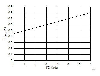
| I2C (ONLY FOR bq51021) | ||||||
| VIL | Input low threshold level SDA | V(PULLUP) = 1.8 V, SDA | 0.4 | V | ||
| VIH | Input high threshold level SDA | V(PULLUP) = 1.8 V, SDA | 1.4 | V | ||
| VIL | Input low threshold level SCL | V(PULLUP) = 1.8 V, SCL | 0.4 | V | ||
| VIH | Input high threshold level SCL | V(PULLUP) = 1.8 V, SCL | 1.4 | V | ||
| I2C speed | Typical | 100 | kHz | |||
7.6 Typical Characteristics
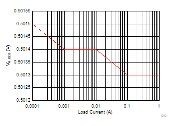
| Temp = 25°C | TX = bq500212A | |