ZHCSCI8 May 2014
PRODUCTION DATA.
- 1 特性
- 2 应用范围
- 3 说明
- 4 简化电路原理图
- 5 修订历史记录
- 6 Pin Configuration and Functions
- 7 Specifications
-
8 Detailed Description
- 8.1 Overview
- 8.2 Functional Block Diagram
- 8.3 Feature Description
- 8.4 Device Functional Modes
- 8.5 Register Maps
-
9 Applications and Implementation
- 9.1 Application Information
- 9.2
Typical Applications
- 9.2.1
WPC Power Supply 5-V Output With 1-A Maximum Current and I2C
- 9.2.1.1 Design Requirements
- 9.2.1.2
Detailed Design Procedure
- 9.2.1.2.1 Output Voltage Set Point
- 9.2.1.2.2 Output and Rectifier Capacitors
- 9.2.1.2.3 Maximum Output Current Set Point
- 9.2.1.2.4 TERM Pin
- 9.2.1.2.5 I2C
- 9.2.1.2.6 Communication Current Limit
- 9.2.1.2.7 Receiver Coil
- 9.2.1.2.8 Series and Parallel Resonant Capacitors
- 9.2.1.2.9 Communication, Boot, and Clamp Capacitors
- 9.2.1.3 Application Performance Plots
- 9.2.2 bq5102x Standalone in System Board or Back Cover
- 9.2.1
WPC Power Supply 5-V Output With 1-A Maximum Current and I2C
- 10Power Supply Recommendations
- 11Layout
- 12器件和文档支持
- 13机械封装和可订购信息
9 Applications and Implementation
9.1 Application Information
The bq5102x device complies with the WPC v1.1 standard. There are several tools available for the design of the system. These tools may be obtained by checking the product page at www.ti.com. The following sections detail how to design a WPC v1.1 mode RX system.
9.2 Typical Applications
9.2.1 WPC Power Supply 5-V Output With 1-A Maximum Current and I2C
 Figure 13. WPC 5-W Schematic Using bq5102x
9.2.1.1 Design Requirements
Table 17. Design Parameters
| DESIGN PARAMETER | EXAMPLE VALUE |
|---|---|
| VOUT | 5 V |
| IOUT MAXIMUM | 1 A |
| MODE | WPC v1.1 |
9.2.1.2 Detailed Design Procedure
To begin the design procedure, start by determining the following:
- Mode of operation – in this case WPC v1.1
- Output voltage
- Maximum output current
9.2.1.2.1 Output Voltage Set Point
The output voltage of the bq5102x device can be set by adjusting a feedback resistor divider network. The resistor divider network is used to set the voltage gain at the VO_REG pin. The device is intended to operate where the voltage at the VO_REG pin is set to 0.5 V. This value is the default setting and can be changed through I2C (for the device bq51021). In Figure 14, R6 and R7 are the feedback network for the output voltage sense.
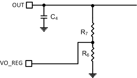 Figure 14. Voltage Gain for Feedback


Choose R7 to be a standard value. In this case, take care to choose R6 and R7 to be large values in order to avoid dissipating excessive power in the resistors, and thereby lowering efficiency.
KVO is set to be 0.5 / 5 = 0.1, choose R7 to be 102 kΩ, and thus R6 to be 11.3 kΩ.
9.2.1.2.2 Output and Rectifier Capacitors
Set C4 between 1 and 4.7 µF. This example uses 1 µF.
Set C3 between 4.7 and 22 µF. This example uses 20 µF.
9.2.1.2.2.1 TMEM
Set C5 to 2.2 µF. In order to determine the bleed off resistor, the WPC transmitters for which the PD_DET is being set for needs to be determined. After the ping timing (time between two consecutive digital pings after EPT charge complete is sent) is determined, the bleedoff resistor can be determined. This example uses TI transmitter EVMs for the use case. In this case, the time between pings is 5 s. To set the time constant using the Equation 8, it is set to 5600 kΩ.
9.2.1.2.3 Maximum Output Current Set Point
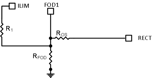 Figure 15. Current Limit Setting for bq5102x
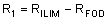
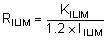
The bq5102x device includes a means of providing hardware overcurrent protection by means of an analog current regulation loop. The hardware current limit provides a level of safety by clamping the maximum allowable output current (for example, a current compliance). The RILIM resistor size also sets the thresholds for the dynamic rectifier levels and thus providing efficiency tuning per each application’s maximum system current. The calculation for the total RILIM resistance is as follows:

The RILIM will allow for the ILIM pin to reach 1.2 V at an output current equal to IILIM. When choosing RILIM, two options are possible.
If the application requires an output current equal to or greater than external ILIM that the circuit is designed for (input current limit on the charger where the RX is delivering power to is higher than the external ILIM), ensure that the downstream charger is capable of regulating the voltage of the input into which the RX device output is tied to by lowering the amount of current being drawn. This will ensure that the RX output does not collapse.
Such behavior is referred to as VIN DPM in TI chargers. Unless such behavior is enabled on the charger, the charger will pull the output of the RX device to ground when the RX device enters current regulation.
If the applications are designed to extract less than the ILIM (1-A maximum), typical designs should leave a design margin of at least 20% so that the voltage at ILIM pin reaches 1.2 V when 20% more than maximum current of the system is drawn from the output of the RX. Such a design would have input current limit on the charger lower than the external ILIM of the RX device.
In both cases, the charger must be capable of regulating the current drawn from the device to allow the output voltage to stay at a reasonable value. This same behavior is also necessary during the WPC V1.1 Communication. See Communication Current Limit for more details. The following calculations show how such a design is achieved:
When referring to the application diagram shown in Figure 15, RILIM is the sum of the R1 and RFOD resistance (that is, the total resistance from the ILIM pin to GND). RFOD is chosen according to the FOD application note that can be obtained by contacting your TI representative. This is used to allow the RX implementation to comply with WPC v1.1 requirements related to received power accuracy.
In many applications, the resistor ROS is needed in order to comply with WPC V1.1 requirements. In such a case, the offset on the FOD pin from the voltage on RFOD can cause a shift in the calculation that can reduce the expected current limit. Therefore, it is always a good idea to check the output current limit after FOD calibration is performed according to the FOD application note. Because the RECT voltage is not deterministic, and depends on transmitter operation to a certain degree, it is not possible to determine R1 with ROS present in a deterministic manner.
In this example, set maximum current for the example to be 1000 mA. Set IILIM = 1.2 A to allow for the 20% margin.
9.2.1.2.4 TERM Pin
The term pin is not used for bq5102x. Leave the pin floating.
9.2.1.2.5 I2C
The I2C lines are used to communicate with the device. To enable the I2C, they can be pulled up to an internal host bus. The device address is 0x6C. I2C is enabled only for the device bq51021.
9.2.1.2.6 Communication Current Limit
Communication current limit allows the device to communicate with the transmitter in an error free manner by decoupling the coil from load transients on the OUT pin during WPC communication. This is done by setting the current limit in a manner that is consistent with Table 4. However, this will require the downstream charger to have a function such as VIN_DPM. In some cases this communication current limit feature is not desirable if the charger does not have this feature. In this design, the user enables the communication current limit by tying the CM_ILIM pin to GND. In the case that this is not needed, the CM_ILIM pin can be tied to OUT pin to disable the communication current limit. In this case, take care that the voltage on the CM_ILIM pin does not exceed the maximum rating of the pin which is 7 V.
9.2.1.2.7 Receiver Coil
The receiver coil design is the most open part of the system design. The choice of the receiver inductance, shape, and materials all intimately influence the parameters themselves in an intertwined manner. This design can be complicated and involves optimizing many different aspects; refer to the user's guide for the EVM (SLUUAX6).
The typical choice of the inductance of the receiver coil for a WPC only 5-V solution is between 8 to 11 µH depending on the mutual inductance between the transmitter coil and the receiver coil.
9.2.1.2.8 Series and Parallel Resonant Capacitors
Resonant capacitors C1 and C2 are set according to WPC specification.
The equations for calculating the values of the resonant capacitors are shown:
9.2.1.2.9 Communication, Boot, and Clamp Capacitors
Set CCOMMx to a value ranging from C1 / 8 to C1 / 3. Note that higher capacitors lower the overall efficiency of the system. Make sure these are X7R ceramic material and have at least a minimum voltage rating of 25 V; TI recommends a minimum voltage rating of 50 V.
Set CBOOTx to be 15 nF. Make sure these are X7R ceramic material and have at least a minimum voltage rating of 25 V; TI recommends a minimum voltage rating of 50 V.
Set CCLAMPx to be 470 nF. Make sure these are X7R ceramic material and have at least a minimum voltage rating of 25 V; TI recommends a minimum voltage rating of 50 V.
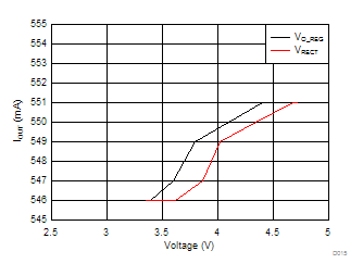
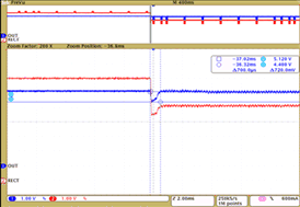
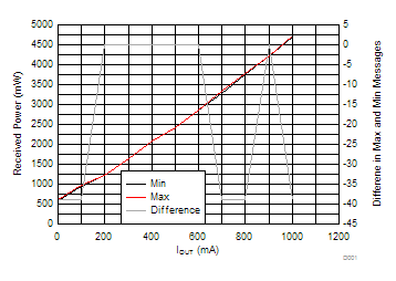
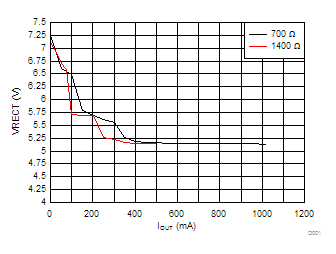
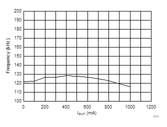
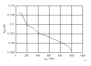
9.2.1.3 Application Performance Plots
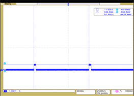
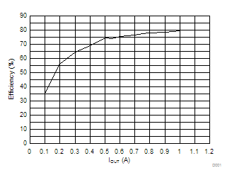
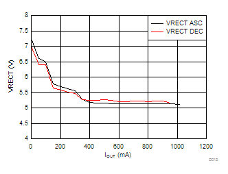
WPC TX
9.2.2 bq5102x Standalone in System Board or Back Cover
When the bq5102x device is implemented as an embedded device on the system board, the EN1 and EN2 pins are the only differences from the previous design using I2C.
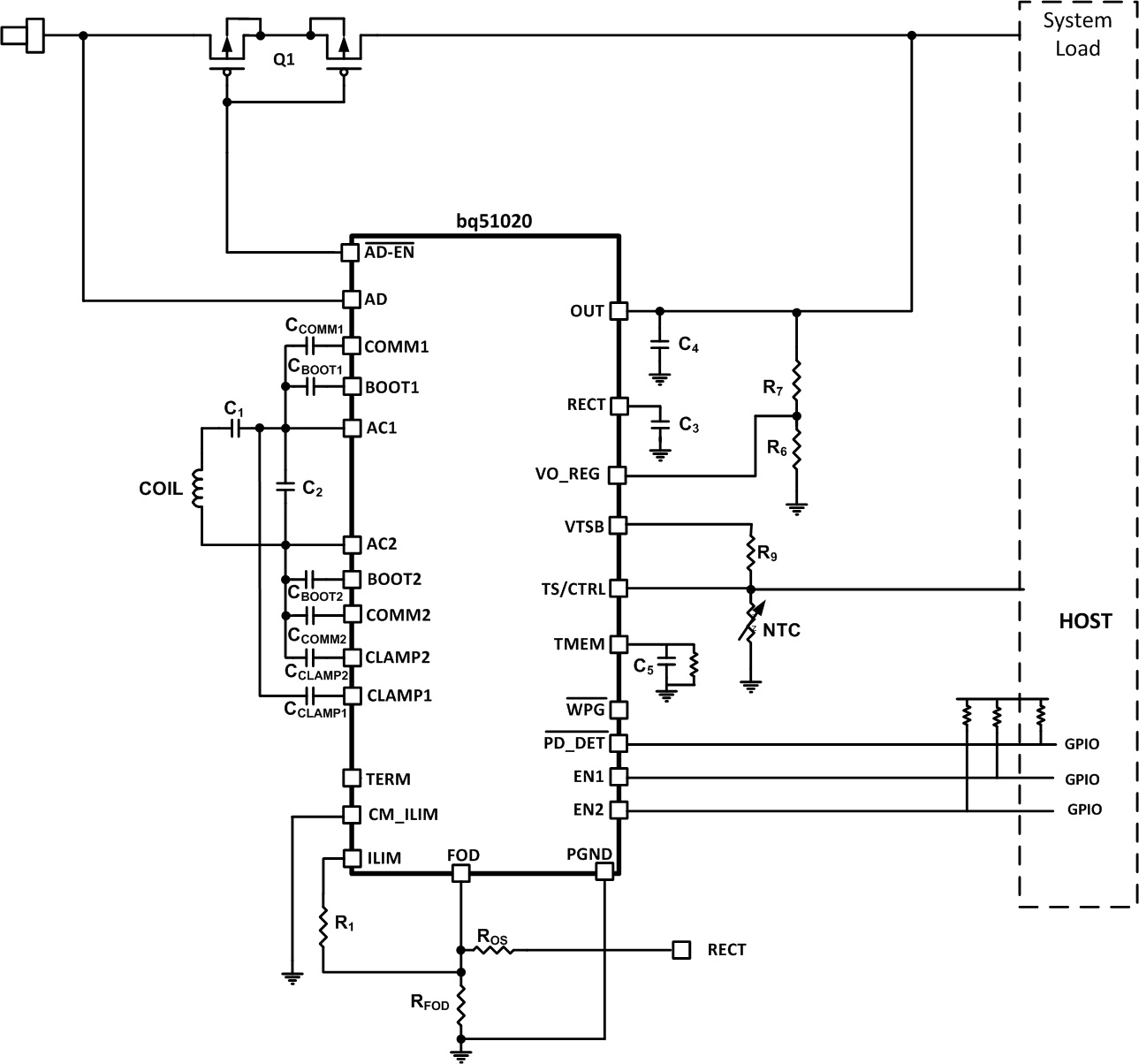 Figure 28. bq5102x Embedded in a System Board
Refer to WPC Power Supply 5-V Output With 1-A Maximum Current and I2C for all design and application details.