ZHCSCI8 May 2014
PRODUCTION DATA.
- 1 特性
- 2 应用范围
- 3 说明
- 4 简化电路原理图
- 5 修订历史记录
- 6 Pin Configuration and Functions
- 7 Specifications
-
8 Detailed Description
- 8.1 Overview
- 8.2 Functional Block Diagram
- 8.3 Feature Description
- 8.4 Device Functional Modes
- 8.5 Register Maps
-
9 Applications and Implementation
- 9.1 Application Information
- 9.2
Typical Applications
- 9.2.1
WPC Power Supply 5-V Output With 1-A Maximum Current and I2C
- 9.2.1.1 Design Requirements
- 9.2.1.2
Detailed Design Procedure
- 9.2.1.2.1 Output Voltage Set Point
- 9.2.1.2.2 Output and Rectifier Capacitors
- 9.2.1.2.3 Maximum Output Current Set Point
- 9.2.1.2.4 TERM Pin
- 9.2.1.2.5 I2C
- 9.2.1.2.6 Communication Current Limit
- 9.2.1.2.7 Receiver Coil
- 9.2.1.2.8 Series and Parallel Resonant Capacitors
- 9.2.1.2.9 Communication, Boot, and Clamp Capacitors
- 9.2.1.3 Application Performance Plots
- 9.2.2 bq5102x Standalone in System Board or Back Cover
- 9.2.1
WPC Power Supply 5-V Output With 1-A Maximum Current and I2C
- 10Power Supply Recommendations
- 11Layout
- 12器件和文档支持
- 13机械封装和可订购信息
11 Layout
11.1 Layout Guidelines
- Keep the trace resistance as low as possible on AC1, AC2, and OUT.
- Detection and resonant capacitors need to be as close to the device as possible.
- COMM, CLAMP, and BOOT capacitors need to be placed as close to the device as possible.
- Via interconnect on GND net is critical for appropriate signal integrity and proper thermal performance.
- High frequency bypass capacitors need to be placed close to RECT and OUT pins.
- ILIM and FOD resistors are important signal paths and the loops in those paths to GND must be minimized.
- AC1 = AC2 = 1.2 A
- OUT = 1 A
- RECT = 100 mA (RMS)
- COMMx = 300 mA
- CLAMPx = 500 mA
- All others can be rated for 10 mA or less
Signal and sensing traces are the most sensitive to noise; the sensing signal amplitudes are usually measured in mV, which is comparable to the noise amplitude. Make sure that these traces are not being interfered by the noisy and power traces. AC1, AC2, BOOT1, BOOT2, COMM1, and COMM2 are the main source of noise in the board. These traces should be shielded from other components in the board. It is usually preferred to have a ground copper area placed underneath these traces to provide additional shielding. Also, make sure they do not interfere with the signal and sensing traces. The PCB should have a ground plane (return) connected directly to the return of all components through vias (two vias per capacitor for power-stage capacitors, one via per capacitor for small-signal components.
For a 1-A fast charge current application, the current rating for each net is as follows:
11.2 Layout Example
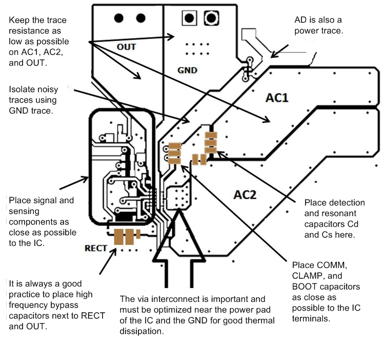 Figure 29. Layout Example for bq5102x