ZHCSEA8A October 2015 – October 2015
PRODUCTION DATA.
7 Detailed Description
7.1 Overview
The principle of wireless power transfer is simply an open-cored transformer consisting of transmitter and receiver coils. The transmitter coil and electronics are typically built into a charger pad and the receiver coil and electronics are typically built into a portable device, such as a smart phone. When the receiver coil is positioned on the transmitter coil, magnetic coupling occurs when the transmitter coil is driven. The flux is coupled into the secondary coil, which induces a voltage and current flows. The secondary voltage is rectified, and power can be transferred effectively to a load, wirelessly. Power transfer can be managed through various closed loop control schemes.
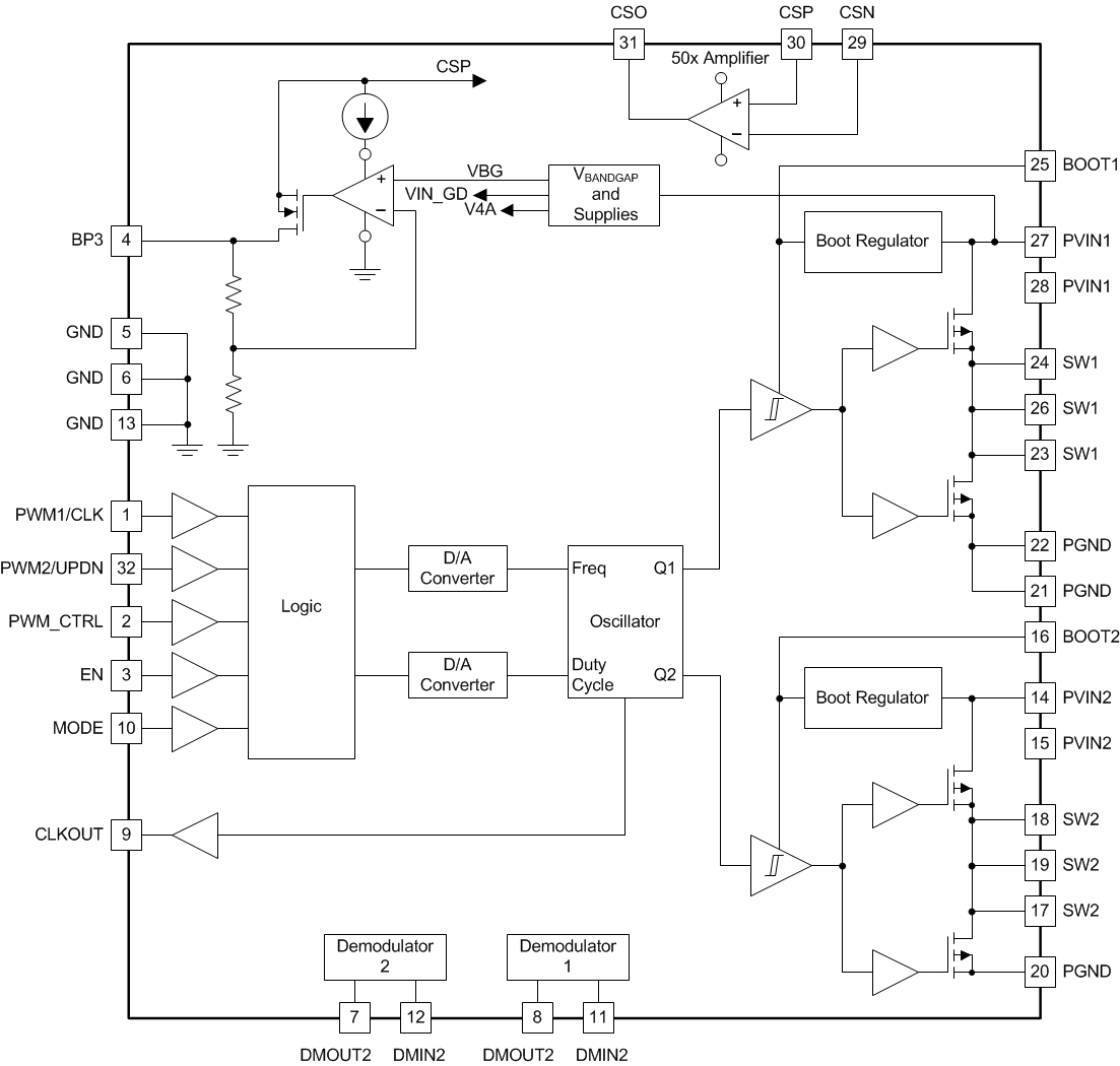
After power is applied and the transmitter device comes out of reset, it will automatically begin the process of detecting and powering a receiver. The bq500511 sends a ping to detect the presence of a receiver on the pad. After a receiver is detected, the bq500511 attempts to establish communication and begin power transfer. The bq500511 is designed to operate with the bq50002 Wireless Power Transmitter Analog Front End to control a full-bridge power stage to drive the primary coil. Through a simple interface the bq500511 instructs the bq50002 how much to increase or decrease power. The full bridge power stage allows for higher power delivery for a given supply voltage.
7.2 Functional Block Diagram

7.3 Feature Description
7.3.1 Demodulator
The embedded demodulator outputs at least one valid bit stream under all modulation conditions that can be used by the accompanied bq500511 controller in order to comply with WPC specification.
More specifically, the WPC worst case condition is defined as the transmitter operating at the minimum modulation level, and the receiver coil is measured by certain x, y and z axis distance to the center of the transmitter coil.
Analog demodulation channel function diagram:
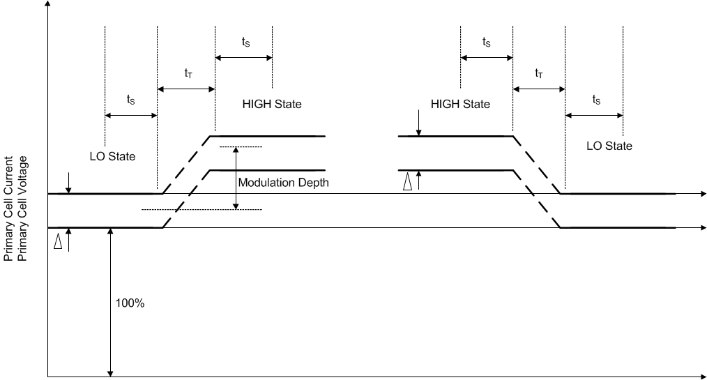
- The diagram below from the WPC spec document explains the concept of Minimum Modulation. The peak-to-peak amplitude difference in TX coil waveform between HI and LO states is 400 mV. With 20-Vpp carrier waveform, and 400-mVpp modulation, with a typical divider it translates to 1 Vpp ±20 mVpp at the input of the demodulator channel.
- The difference of the amplitude of the primary cell voltage in the HI and LO state is at least 200 mV.
During a transition the primary cell current and primary cell voltages are undefined. See Figure 3.
 Figure 3. Amplitude Modulation of the Power Signal
7.3.2 PWM Control
7.3.2.1 PWM_CTRL Input
bq50002 operates in two modes:
Direct PWM Control Mode and Self Switching. The mode of operation is set by the state of PWM_CTRL input when EN=HIGH. This is intended for control by bq500511.
7.3.2.2 PWM1, PWM2
bq50002 passes external PWM inputs to drive gate drivers when the following conditions hold:
- EN pin is HIGH
- PWM_CTRL pin is HIGH
- Typical Dead Time shall be better than 20 ns. Minimum PWM input pulse duration that changes SW output should be less than 50 ns.
7.3.2.3 Self-Switching
bq50002 follows the commands from the controller to adjust the internal oscillator frequency up or down to adjust output power levels when the following conditions apply:
- PWM_CTRL pin is LOW
- PWM1/CLK_IN behaves as CLK_IN pin. The CLK_IN rising edge triggers frequency increase or decrease by one step based on the state of PWM2/UP_DN pin.
- Self-switching starts at F=175 kHz when PWM_CTRL state changes from HIGH to LOW. Operating frequency changes are based on the inputs of UP_DN, CLK_IN and MODE.
- The CLK_OUT pin outputs 3.3V logic level with frequency equal in value to the current switching frequency. The rising edge of this signal coincides with the rising edge of the SW1 waveform. The duty factor of the signal on CLK_OUT pin is 50%.
- bq50002 increases the frequency (reduces delivered power) if:
- PWM_CTRL pin is LOW
- MODE pin is LOW
- UP_DN pin is LOW
- CLK_IN pin changes its state from LOW to HIGH (rising edge)
- bq50002 decreases the frequency (increases delivered power) if:
- PWM_CTRL pin is LOW
- MODE pin is LOW
- UP_DN pin is HIGH
- CLK_IN pin changes its state from LOW to HIGH (rising edge)
7.3.2.4 Duty Cycle Adjustment
bq50002 follows the commands from the controller to adjust the internal oscillator duty cycle up or down to adjust power output levels when the following conditions hold:
- The internal clock is set to the highest frequency tap, 205 kHz
- PWM_CTRL pin is LOW
- MODE pin is HIGH
- bq50002 decreases the duty cycle (reduces delivered power) if:
- The internal clock is set to the highest frequency tap, 205 kHz or at frequency at which MCU commands MODE = 1
- PWM_CTRL pin is LOW
- MODE pin is HIGH
- UP_DN is LOW
- CLK_IN pin changes state from LOW to HIGH (rising edge)
- bq50002 ignores CLK_IN signals when minimum duty factor position of 10% is reached
- bq50002 increases the duty cycle (increases delivered power) if:
- The internal clock is set to the highest frequency tap, 205 kHz at frequency at which MCU commands MODE = 1
- PWM_CTRL pin is LOW
- MODE pin is HIGH
- UP_DN is HIGH
- CLK_IN pin changes state from LOW to HIGH (rising edge)
- bq50002 ignores CLK_IN signals when maximum duty factor position of 50% is reached. bq50002 will resume clock frequency adjustment mode only when the duty cycle adjustment has reached the 50% state and MODE=0.
7.3.3 Current Sense Amplifier
To support foreign object detection (FOD), bq50002 senses the average input current to the device. The integrated current sense amplifier has voltage gain of 50.
7.3.4 Voltage Regulator
bq50002 has an integrated low-dropout (LDO) voltage regulator which supplies power to the companion bq500511 controller. The BP3 pin supplies a regulated 3-V voltage supply and should have a 2.2-µF capacitor tied to GND.
7.4 Device Functional Modes
7.4.1 Power Transfer
Power transfer efficiency and robustness depends on coil coupling. Coupling depends on the distance between coils, alignment, coil dimensions, coil materials, number of turns, magnetic shielding, impedance matching, frequency. Most importantly, the receiver and transmitter coils must be aligned for best coupling and efficient power transfer. The smaller the space between the coils is, the better the coupling. Shielding is added as a backing to both the transmitter and receiver coils to direct the magnetic field to the coupled zone. Magnetic fields outside the coupled zone do not transfer power. Thus, shielding also serves to contain the fields to avoid coupling to other adjacent system components.
Regulation can be achieved by controlling any one of the coil coupling parameters. However, for WPC compatibility, the transmitter-side coils and capacitance are specified and the resonant frequency point is fixed. In the bq500511/bq50002 system power transfer is regulated by changing the operating frequency between 110 kHz to 205 kHz. The higher the frequency, the further from resonance and the lower the power. Duty cycle remains constant at 50% throughout the power band and is reduced only once 205 kHz is reached.
7.4.1.1 Dynamic Power Limiting™
Dynamic Power Limiting™ (DPL) allows operation from a 5-V supply with limited current capability (such as a USB port). When the input voltage is observed drooping, the output power is dynamically limited to reduce the load and provides margin relative to the supply’s capability.
Anytime the DPL control loop is regulating the operating point of the transmitter, the LED will indicate that DPL is active. The LED color and flashing pattern are determined by the LED Table. If the receiver sends a Control Error Packet (CEP) with a negative value, (for example, to reduce power to the load), the bq500511 in DPL mode will return to normal operation and respond to this CEP via the standard WPC control loop behavior.
7.4.2 Communication
Communication within the WPC v1.2 specification is from the receiver to the transmitter. For example, in order to regulate the output of the transmitter, the receiver sends messages requesting the transmitter to increase or decrease power. The receiver communicates by modulating the rectifier voltage and using amplitude modulation (AM) sends packets of information to the transmitter. A packet is comprised of a preamble, a header, the actual message, and a checksum, as defined by the WPC standard.
The receiver sends a packet by modulating an impedance network. This AM signal reflects back as a change in the voltage amplitude on the transmitter coil. In the bq500511/bq50002 system, the bq50002 performs the demodulation function and passes a digitized version of the message to the bq500511 where the message is decoded and processed. For example in response to a Control Error Packet, the bq500511 calculates the required change in output power and in turn controls the bq50002 through the CLK_OUT, UP_DOWN, and MODE pins to adjust the operating point and thus its output power.
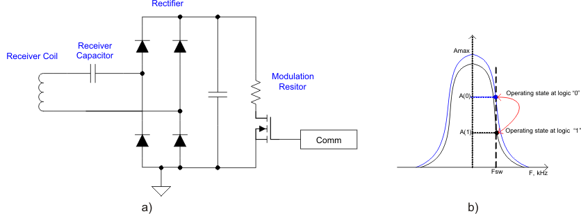
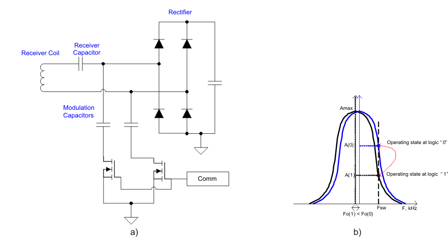
The modulation impedance network on the receiver can either be resistive or capacitive. Figure 4 shows the resistive modulation approach, where a resistor is periodically added to the load, resulting in an amplitude change in the transmitter voltage. Figure 5 shows the corresponding capacitive modulation approach.
 Figure 4. Receiver Resistive Modulation Circuit
 Figure 5. Receiver Capacitive Modulation Circuit