ZHCSEA8A October 2015 – October 2015
PRODUCTION DATA.
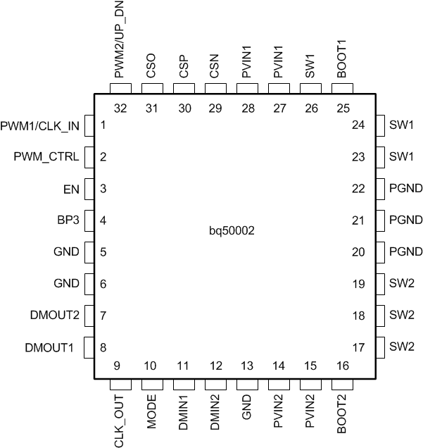
5 Pin Configuration and Functions
RHB Package
32-Pin QFN
Top View

Pin Functions
| PIN | I/O | DESCRIPTION | |
|---|---|---|---|
| NAME | NO. | ||
| BOOT1 | 25 | I/O | Positive supply rail for the high-side gate driver. Connect a 0.1-µF ceramic capacitor between the BOOT1 and SW1 pins. |
| BOOT2 | 16 | I/O | Positive supply rail for the high-side gate driver. Connect a 0.1-µF ceramic capacitor between the BOOT2 and SW2 pins. |
| BP3 | 4 | O | LDO output. Tie with 2.2-µF capacitor to GND. For use by bq500511 only. |
| CLK_OUT | 9 | O | Internal oscillator clock out signal. |
| CSN | 29 | I | Current sense amplifier negative input. |
| CSO | 31 | O | Current sense amplifier output. For use by bq500511 only. |
| CSP | 30 | I | Current sense amplifier positive input. Connect current sense resistor as close as possible to this pin. This also serves as the quiet node for power supply input. |
| DMIN1 | 11 | I | Modulated signal from coil for DEMOD CHAN1. |
| DMIN2 | 12 | I | Modulated signal from coil for DEMOD CHAN2. |
| DMOUT1 | 8 | O | Demodulated 2-kHz signal from CHAN1. For use by bq500511 only. |
| DMOUT2 | 7 | O | Demodulated 2-kHz signal from CHAN2. For use by bq500511 only. |
| EN | 3 | I | Enable pin with a weak internal pull-down. Float or pull below 1.5 V to disable gate driver, demodulation and current sense. Pull above 2.2 V to enable gate driver. Used by bq500511 to enter and leave standby mode for the transmitter. |
| GND | 5 | – | Signal ground for the ground-referenced logic. All signal level circuits should be referenced to this pin unless otherwise noted. |
| GND | 6 | – | Signal ground for the ground-referenced logic. All signal level circuits should be referenced to this pin unless otherwise noted. |
| GND | 13 | – | Signal ground for the ground-referenced logic. All signal level circuits should be referenced to this pin unless otherwise noted. |
| MODE | 10 | I | MODE pin with a weak internal pull-down. Float, or pull below 1.5 V to enable frequency control of the internally generated PWM signal. Pull above 2.2 V to enable pulse width control of the internally generated PWM signal. Used by bq500511 to select the control method for power control |
| PGND | 20 | – | Power ground for the ground-referenced power stage. Connect to GND. |
| PGND | 21 | – | Power ground for the ground-referenced power stage. Connect to GND. |
| PGND | 22 | – | Power ground for the ground-referenced power stage. Connect to GND. |
| PVIN1 | 27 | I | DC input voltage for half-bridge MOSFET. Bypass with 22-µF ceramic capacitor to GND. |
| PVIN1 | 28 | I | DC input voltage for half-bridge MOSFET. Bypass with 22-µF ceramic capacitor to GND. |
| PVIN2 | 14 | I | DC input voltage for half-bridge MOSFET. Bypass with 22-µF ceramic capacitor to GND. |
| PVIN2 | 15 | I | DC input voltage for half-bridge MOSFET. Bypass with 22-µF ceramic capacitor to GND. |
| PWM_CTRL | 2 | I | PWM_CTRL pin with a weak internal pull-down. Controlled by bq500511 (SLUSCD3) for system power delivery control. |
| PWM1/CLK_IN | 1 | I | PWM1/CLK_IN pin with a weak internal pull-down. Controlled by bq500511 (SLUSCD3) for system power delivery control. |
| PWM2/UP_DN | 32 | I | PWM2/UP_DN pin with a weak internal pull-down. Controlled by bq500511 (SLUSCD3) for system power delivery control. |
| SW1 | 23 | O | Switch node of the half-bridge MOSFETs. Connect to TX coil. |
| SW1 | 24 | O | Switch node of the half-bridge MOSFETs. Connect to TX coil. |
| SW1 | 26 | O | Switch node of the half-bridge MOSFETs . Connect to TX coil. |
| SW2 | 17 | O | Switch node of the half-bridge MOSFETs. Connect to resonant capacitor. |
| SW2 | 18 | O | Switch node of the half-bridge MOSFETs. Connect to resonant capacitor. |
| SW2 | 19 | O | Switch node of the half-bridge MOSFETs. Connect to resonant capacitor. |