ZHCSRG2G May 2001 – December 2022 BQ2057C
PRODUCTION DATA
- 1 特性
- 2 应用
- 3 说明
- 4 Revision History
- 5 说明(续)
- 6 Device Comparison Table
- 7 Pin Configuration and Functions
- 8 Specifications
- 9 Detailed Description
-
10Application and Implementation
- 10.1
Application Information
- 10.1.1 Functional Description
- 10.1.2 Qualification and Precharge
- 10.1.3 Current Regulation Phase
- 10.1.4 Voltage Regulation Phase
- 10.1.5 Charge Termination and Recharge
- 10.1.6 Battery Temperature Monitoring
- 10.1.7 Charge Inhibit Function
- 10.1.8 Charge Status Indication
- 10.1.9 Low-power Sleep Mode
- 10.1.10 Selecting an External Pass-Transistor
- 10.1.11 Selecting Input Capacitor
- 10.1.12 Selecting Output Capacitor
- 10.1.13 Automatic Charge-rate Compensation
- 10.2 Typical Application
- 10.1
Application Information
- 11Power Supply Recommendations
- 12Layout
- 13Device and Documentation Support
- 14Mechanical, Packaging, and Orderable Information
封装选项
请参考 PDF 数据表获取器件具体的封装图。
机械数据 (封装 | 引脚)
- D|8
- DGK|8
- PW|8
散热焊盘机械数据 (封装 | 引脚)
订购信息
10.1.13 Automatic Charge-rate Compensation
To reduce charging time, the BQ2057 uses the proprietary AutoComp technique to compensate safely for internal impedance of the battery pack. The AutoComp feature is disabled by connecting the COMP pin to VCC in high-side current-sensing configuration, and to VSS in low-side current-sensing configuration. The COMP pin must not be left floating.
Figure 10-12 outlines the major components of a single-cell Li-Ion battery pack. The Li-Ion battery pack consists of a cell, protection circuit, fuse, connector, current sense-resistors, and some wiring. Each of these components contains some resistance. Total impedance of the battery pack is the sum of the minimum resistances of all battery-pack components. Using the minimum resistance values reduces the odds for overcompensating. Overcompensating may activate the safety circuit of the battery pack.
 Figure 10-12 Typical
Components of a Single-Cell Li-Ion Pack
Figure 10-12 Typical
Components of a Single-Cell Li-Ion PackCompensation is achieved through input pin COMP (Figure 10-13). A portion of the current-sense voltage, presented through this pin, is scaled by a factor of G(COMP) and summed with the regulation threshold, VO(REG). This process increases the output voltage to compensate for the battery pack’s internal impedance and for undesired voltage drops in the circuit.
AutoComp setup requires the following information:
- Total impedance of battery pack (Z(PACK))
- Maximum charging current (I(REG))
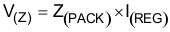
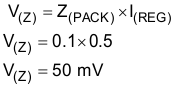
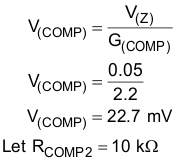
The voltage drop across the internal impedance of battery pack, V(Z), can then be calculated using Equation 13:
The required compensation is then calculated using Equation 14:
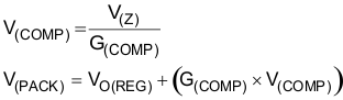
Where V(COMP) is the voltage on COMP pin. This voltage is referenced to VCC in high-side current sensing configuration and to VSS for low-side sensing. V(PACK) is the voltage across the battery pack.
The values of R(COMP1) and R(COMP2) can be calculated using Equation 15:
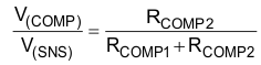
 Figure 10-13 AutoComp
Circuits
Figure 10-13 AutoComp
CircuitsThe following example illustrates these calculations:
Assume Z(PACK) = 100 mΩ, I(REG) = 500 mA, high-side current sensing BQ2057C
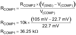
Use the closest standard value (36.0 kΩ) for RCOMP1.