ZHCSAT7H December 2012 – October 2014 AFE4490
PRODUCTION DATA.
- 1 特性
- 2 应用范围
- 3 说明
- 4 修订历史记录
- 5 Device Comparison Table
- 6 Pin Configuration and Functions
- 7 Specifications
- 8 Detailed Description
- 9 Applications and Implementation
- 10Power-Supply Recommendations
- 11Layout
- 12器件和文档支持
- 13机械封装和可订购信息
8 Detailed Description
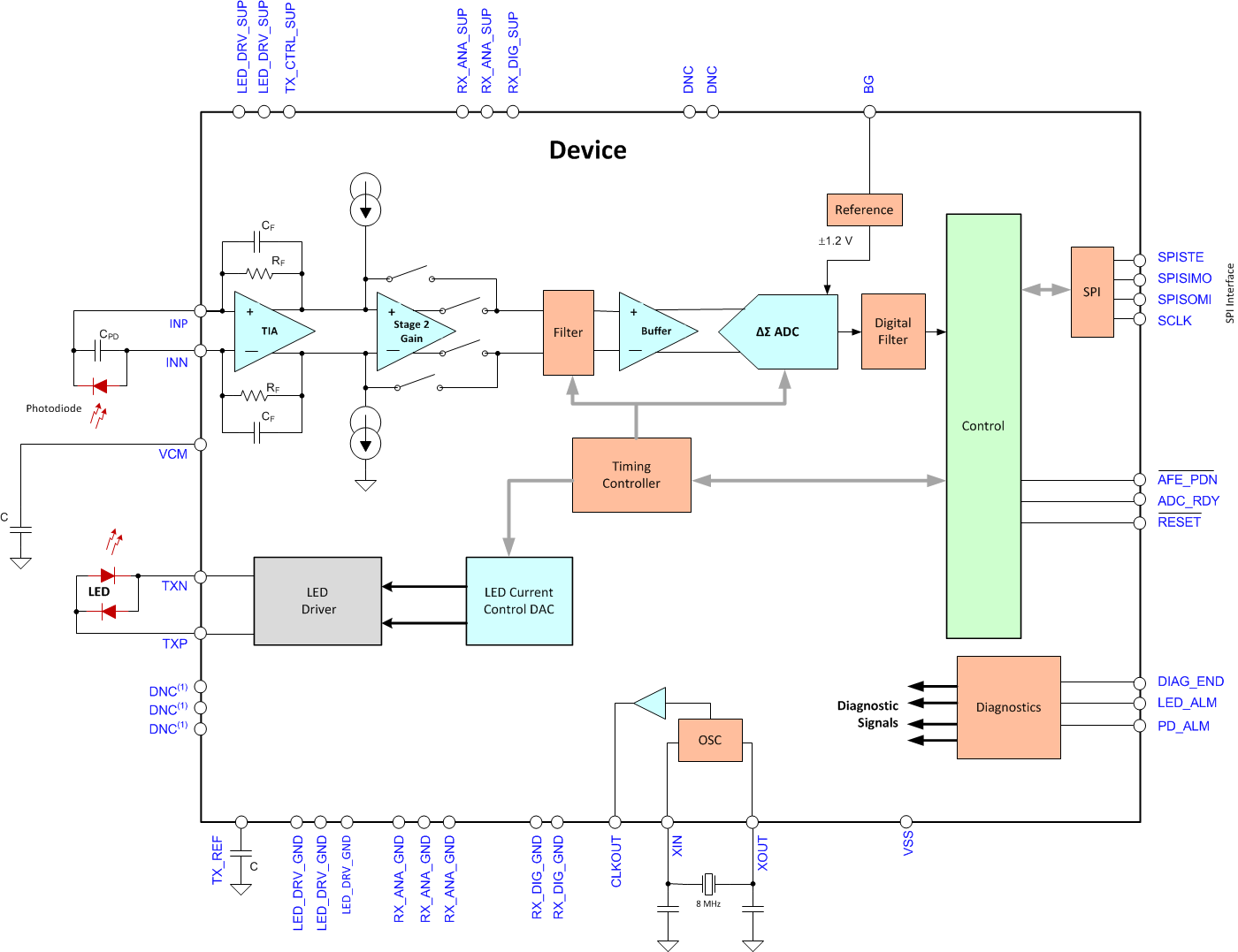
8.1 Overview
The AFE4490 is a complete analog front-end (AFE) solution targeted for pulse-oximeter applications. The device consists of a low-noise receiver channel, an LED transmit section, and diagnostics for sensor and LED fault detection. To ease clocking requirements and provide the low-jitter clock to the AFE, an oscillator is also integrated that functions from an external crystal. The device communicates to an external microcontroller or host processor using an SPI interface. The Functional Block Diagram section provides a detailed block diagram for the device. The blocks are described in more detail in the following sections.
8.3 Feature Description
8.3.1 Receiver Channel
This section describes the receiver channel functionality.
8.3.1.1 Receiver Front-End
The receiver consists of a differential current-to-voltage (I-V) transimpedance amplifier that converts the input photodiode current into an appropriate voltage, as shown in Figure 55. The feedback resistor of the amplifier (RF) is programmable to support a wide range of photodiode currents. Available RF values include: 1 MΩ, 500 kΩ,
250 kΩ, 100 kΩ, 50 kΩ, 25 kΩ, and 10 kΩ.
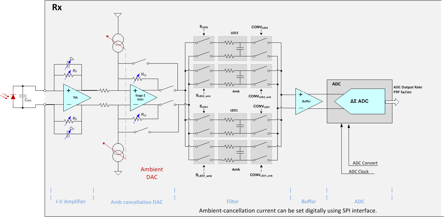
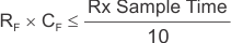
The RF amplifier and the feedback capacitor (CF) form a low-pass filter for the input signal current. Always ensure that the low-pass filter RC time constant has sufficiently high bandwidth (as shown by Equation 1) because the input current consists of pulses. For this reason, the feedback capacitor is also programmable. Available CF values include: 5 pF, 10 pF, 25 pF, 50 pF, 100 pF, and 250 pF. Any combination of these capacitors can also be used.
The output voltage of the I-V amplifier includes the pleth component (the desired signal) and a component resulting from the ambient light leakage. The I-V amplifier is followed by the second stage, which consists of a current digital-to-analog converter (DAC) that sources the cancellation current and an amplifier that gains up the pleth component alone. The amplifier has five programmable gain settings: 0 dB, 3.5 dB, 6 dB, 9.5 dB, and
12 dB. The gained-up pleth signal is then low-pass filtered (500-Hz bandwidth) and buffered before driving a 22-bit ADC. The current DAC has a cancellation current range of 10 µA with 10 steps (1 µA each). The DAC value can be digitally specified with the SPI interface. Using ambient compensation with the ambient DAC allows the dc-biased signal to be centered to near mid-point of the amplifier (±0.9 V). Using the gain of the second stage allows for more of the available ADC dynamic range to be used.
The output of the ambient cancellation amplifier is separated into LED2 and LED1 channels. When LED2 is on, the amplifier output is filtered and sampled on capacitor CR. Similarly, the LED1 signal is sampled on the CLED1 capacitor when LED1 is ON. In between the LED2 and LED1 pulses, the idle amplifier output is sampled to estimate the ambient signal on capacitors CLED2_amb and CLED1_amb.
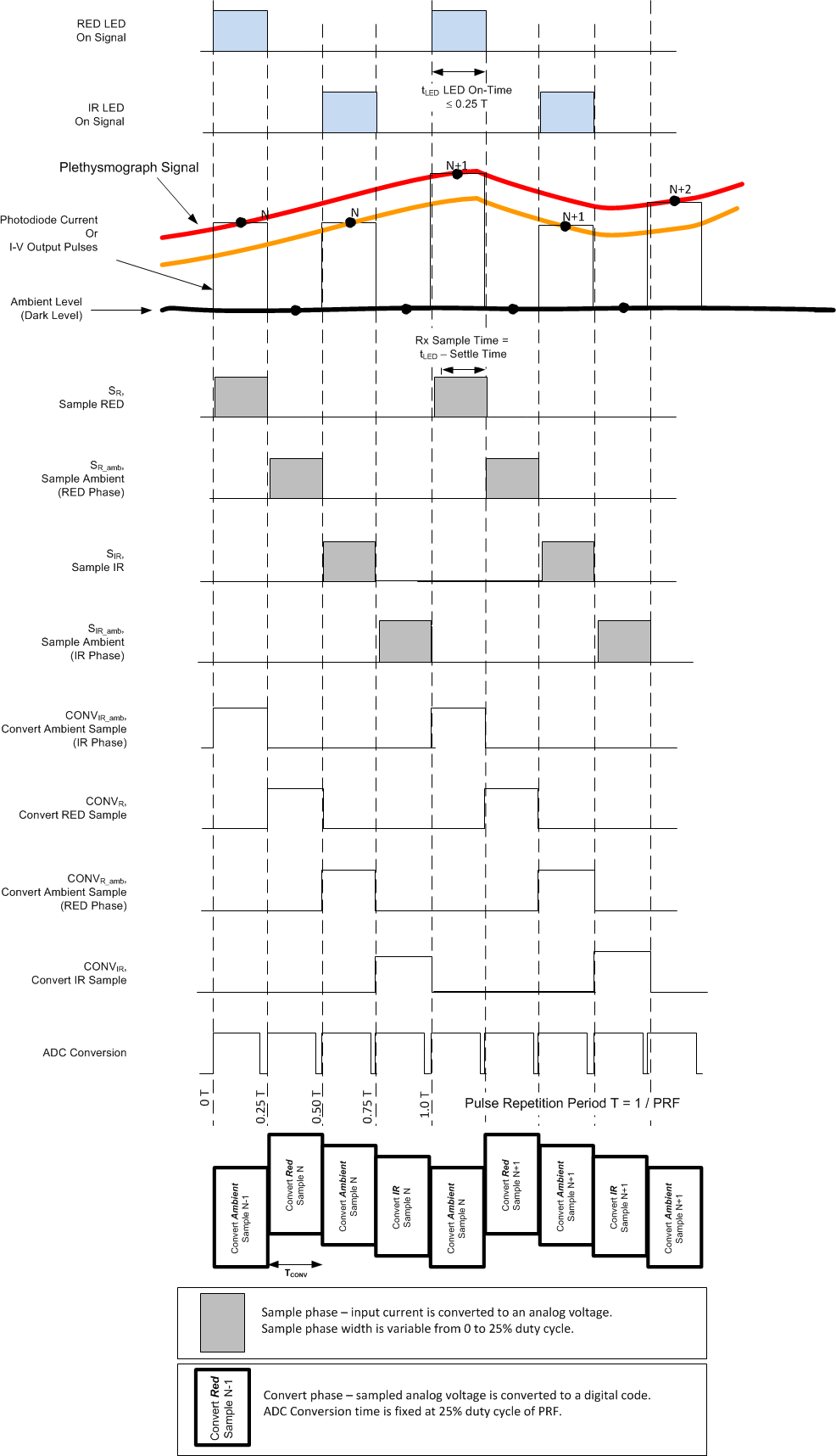
The sampling duration is termed the Rx sample time and is programmable for each signal, independently. Sampling can start after the I-V amplifier output is stable (to account for LED and cable settling times). The Rx sample time is used for all dynamic range calculations; the minimum time supported is 50 µs.
A single, 22-bit ADC converts the sampled LED2, LED1, and ambient signals sequentially. Each conversion takes a maximum of 25% of the pulse repetition period (PRP) and provides a single digital code at the ADC output. As discussed in the Receiver Timing section, the conversions are staggered so that the LED2 conversion starts after the end of the LED2 sample phase, and so on. This configuration also means that the Rx sample time for each signal is no greater than 25% of the pulse repetition period.
Note that four data streams are available at the ADC output (LED2, LED1, ambient LED2, and ambient LED1) at the same rate as the pulse repetition frequency. The ADC is followed by a digital ambient subtraction block that additionally outputs the (LED2 – ambient LED2) and (LED1 – ambient LED1) data values.
8.3.1.2 Ambient Cancellation Scheme
The receiver provides digital samples corresponding to ambient duration. The host processor (external to the AFE) can use these ambient values to estimate the amount of ambient light leakage. The processor must then set the value of the ambient cancellation DAC using the SPI, as shown in Figure 56.
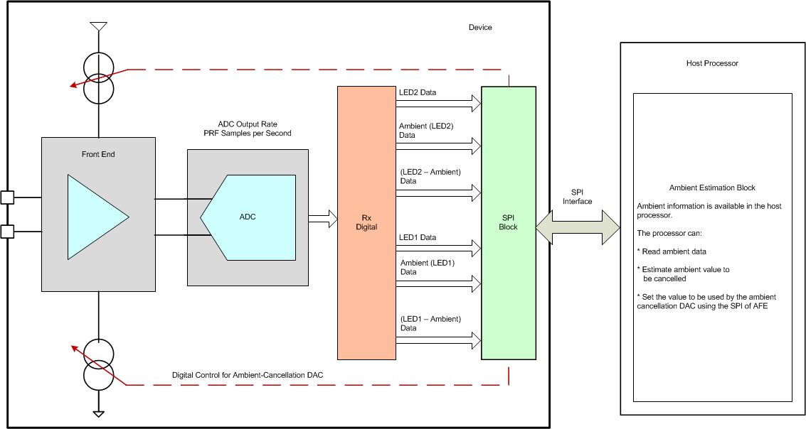 Figure 56. Ambient Cancellation Loop (Closed by the Host Processor)
Using the set value, the ambient cancellation stage subtracts the ambient component and gains up only the pleth component of the received signal, as shown in Figure 57. The amplifier gain is programmable to 0 dB, 3.5 dB,
6 dB, 9.5 dB, and 12 dB.
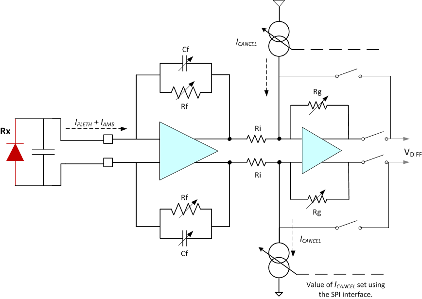 Figure 57. Front-End (I-V Amplifier and Cancellation Stage)
The differential output of the second stage is VDIFF, as given by Equation 2:
where
- RI = 100 kΩ,
- IPLETH = photodiode current pleth component,
- IAMB = photodiode current ambient component, and
- ICANCEL = the cancellation current DAC value (as estimated by the host processor).
RG values with various gain settings are listed in Table 1.
Table 1. RG Values
| RG (dB) | GAIN (kΩ) |
|---|---|
| 0 (x1) | 100 |
| 3.5 (x1.5) | 150 |
| 6 (x2) | 200 |
| 9.5 (x3) | 300 |
| 12 (x4) | 400 |
8.3.1.3 Receiver Control Signals
LED2 sample phase (SLED2): When this signal is high, the amplifier output corresponds to the LED2 on-time. The amplifier output is filtered and sampled into capacitor CLED2. To avoid settling effects resulting from the LED or cable, program SLED2 to start after the LED turns on. This settling delay is programmable.
Ambient sample phase (SLED2_amb): When this signal is high, the amplifier output corresponds to the LED2 off-time and can be used to estimate the ambient signal (for the LED2 phase). The amplifier output is filtered and sampled into capacitor CLED2_amb.
LED1 sample phase (SLED1): When this signal is high, the amplifier output corresponds to the LED1 on-time. The amplifier output is filtered and sampled into capacitor CLED1. To avoid settling effects resulting from the LED or cable, program SLED1 to start after the LED turns on. This settling delay is programmable.
Ambient sample phase (SLED1_amb): When this signal is high, the amplifier output corresponds to the LED1 off-time and can be used to estimate the ambient signal (for the LED1 phase). The amplifier output is filtered and sampled into capacitor CLED1_amb.
LED2 convert phase (CONVLED2): When this signal is high, the voltage sampled on CLED2 is buffered and applied to the ADC for conversion. The conversion time duration is always 25% of the pulse repetition period. At the end of the conversion, the ADC provides a single digital code corresponding to the LED2 sample.
Ambient convert phases (CONVLED2_amb, CONVLED1_amb): When this signal is high, the voltage sampled on CLED2_amb (or CLED1_amb) is buffered and applied to the ADC for conversion. The conversion time duration is always 25% of the pulse repetition period. At the end of the conversion, the ADC provides a single digital code corresponding to the ambient sample.
LED1 convert phase (CONVLED1): When this signal is high, the voltage sampled on CLED1 is buffered and applied to the ADC for conversion. The conversion time duration is always 25% of the pulse repetition period. At the end of the conversion, the ADC provides a single digital code corresponding to the LED1 sample.
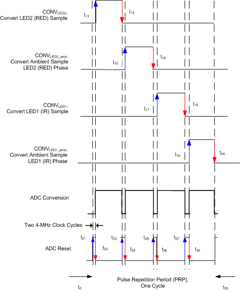
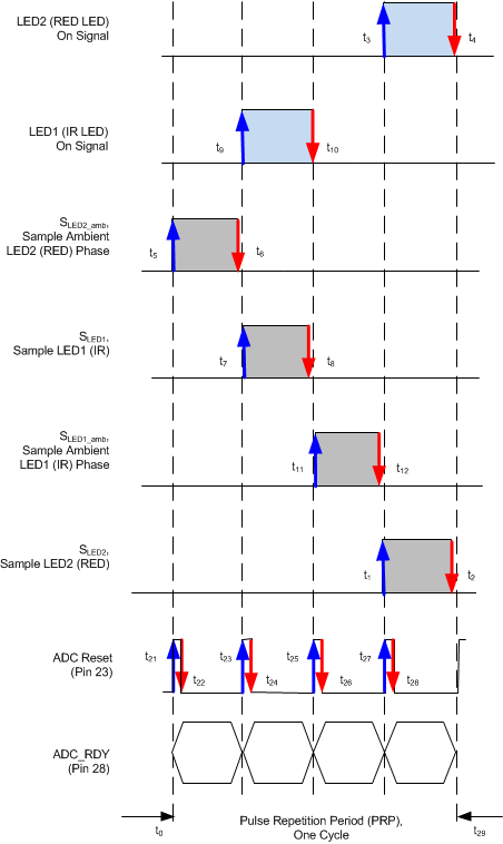
8.3.1.4 Receiver Timing
See Figure 58 for a timing diagram detailing the control signals related to the LED on-time, Rx sample time, and the ADC conversion times for each channel.
8.3.2 Clocking and Timing Signal Generation
The crystal oscillator generates a master clock signal using an external 8-MHz crystal. A divide-by-2 block converts the 8-MHz clock to 4 MHz, which is used by the AFE to operate the timer modules, ADC, and diagnostics. The 4-MHz clock is buffered and output from the AFE in order to clock an external microcontroller. The clocking functionality is shown in Figure 59.
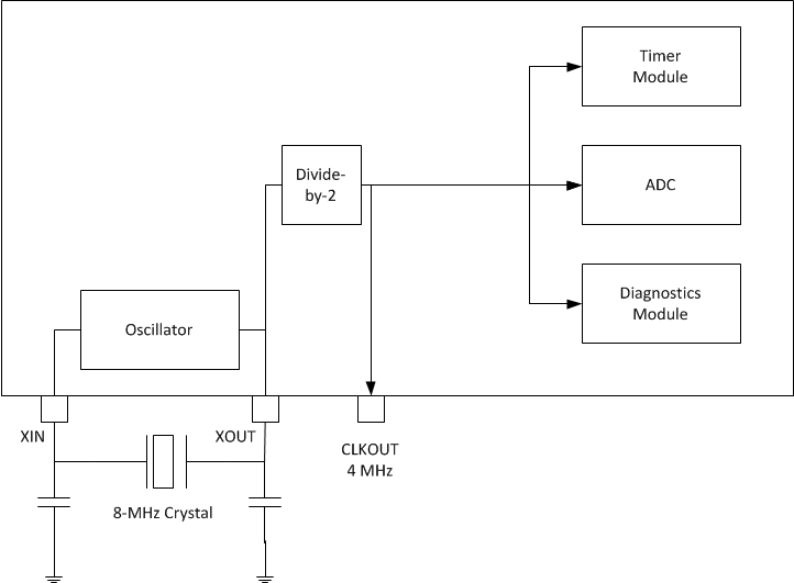 Figure 59. AFE Clocking
8.3.3 Timer Module
See Figure 60 for a timing diagram detailing the various timing edges that are programmable using the timer module. The rising and falling edge positions of 11 signals can be controlled. The module uses a single 16-bit counter (running off of the 4-MHz clock) to set the time-base.
All timing signals are set with reference to the pulse repetition period (PRP). Therefore, a dedicated compare register compares the 16-bit counter value with the reference value specified in the PRF register. Every time that the 16-bit counter value is equal to the reference value in the PRF register, the counter is reset to '0'.
For the 11 signals in Figure 58, the start and stop edge positions are programmable with respect to the PRF period. Each signal uses a separate timer compare module that compares the counter value with preprogrammed reference values for the start and stop edges. All reference values can be set using the SPI interface.
When the counter value equals the start reference value, the output signal is set. When the counter value equals the stop reference value, the output signal is reset. Figure 61 shows a diagram of the timer compare register. With a 4-MHz clock, the edge placement resolution is 0.25 µs. The ADC conversion signal requires four pulses in each PRF clock period. The 11th timer compare register uses four sets of start and stop registers to control the ADC conversion signal.
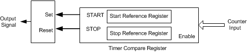 Figure 61. Compare Register
The ADC conversion signal requires four pulses in each PRF clock period. Timer compare register 11 uses four sets of start and stop registers to control the ADC conversion signal, as shown in Figure 62.
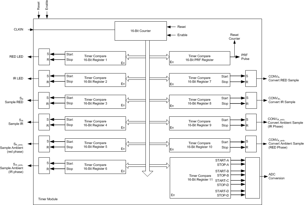 Figure 62. Timer Module
8.3.3.1 Using the Timer Module
The timer module registers can be used to program the start and end instants in units of 4-MHz clock cycles. These timing instants and the corresponding registers are listed in Table 2.
Note that the device does not restrict the values in these registers; thus, the start and end edges can be positioned anywhere within the pulse repetition period. Care must be taken by the user to program suitable values in these registers to avoid overlapping the signals and to make sure none of the edges exceed the value programmed in the PRP register. Writing the same value in the start and end registers results in a pulse duration of one clock cycle. The following steps describe the timer sequencing configuration:
- With respect to the start of the PRP period (indicated by timing instant t0 in Figure 63 and Figure 64), the sequence of conversions must be followed in order: convert LED2 → LED2 ambient → LED1 → LED1 ambient.
- Also, starting from t0, the sequence of sampling instants must be staggered with respect to the respective conversions as follows: sample LED2 ambient → LED1 → LED1 ambient → LED2.
- Finally, align the edges for the two LED pulses with the respective sampling instants.
Table 2. Clock Edge Mapping to SPI Registers
| TIME INSTANT (See Figure 63 and Figure 64) | DESCRIPTION | CORRESPONDING REGISTER ADDRESS AND REGISTER BITS | EXAMPLE(1) (Decimal) |
|---|---|---|---|
| t0 | Start of pulse repetition period | No register control | — |
| t1 | Start of sample LED2 pulse | Sample LED2 start count (bits 15-0 of register 01h) | 6050 |
| t2 | End of sample LED2 pulse | Sample LED2 end count (bits 15-0 of register 02h) | 7998 |
| t3 | Start of LED2 pulse | LED2 start count (bits 15-0 of register 03h) | 6000 |
| t4 | End of LED2 pulse | LED2 end count (bits 15-0 of register 04h) | 7999 |
| t5 | Start of sample LED2 ambient pulse | Sample ambient LED2 start count (bits 15-0 of register 05h) | 50 |
| t6 | End of sample LED2 ambient pulse | Sample ambient LED2 end count (bits 15-0 of register 06h) | 1998 |
| t7 | Start of sample LED1 pulse | Sample LED1 start count (bits 15-0 of register 07h) | 2050 |
| t8 | End of sample LED1 pulse | Sample LED1 end count (bits 15-0 of register 08h) | 3998 |
| t9 | Start of LED1 pulse | LED1 start count (bits 15-0 of register 09h) | 2000 |
| t10 | End of LED1 pulse | LED1 end count (bits 15-0 of register 0Ah) | 3999 |
| t11 | Start of sample LED1 ambient pulse | Sample ambient LED1 start count (bits 15-0 of register 0Bh) | 4050 |
| t12 | End of sample LED1 ambient pulse | Sample ambient LED1 end count (bits 15-0 of register 0Ch) | 5998 |
| t13 | Start of convert LED2 pulse | LED2 convert start count (bits 15-0 of register 0Dh) Must start one AFE clock cycle after the ADC reset pulse ends. |
4 |
| t14 | End of convert LED2 pulse | LED2 convert end count (bits 15-0 of register 0Eh) | 1999 |
| t15 | Start of convert LED2 ambient pulse | LED2 ambient convert start count (bits 15-0 of register 0Fh) Must start one AFE clock cycle after the ADC reset pulse ends. |
2004 |
| t16 | End of convert LED2 ambient pulse | LED2 ambient convert end count (bits 15-0 of register 10h) | 3999 |
| t17 | Start of convert LED1 pulse | LED1 convert start count (bits 15-0 of register 11h) Must start one AFE clock cycle after the ADC reset pulse ends. |
4004 |
| t18 | End of convert LED1 pulse | LED1 convert end count (bits 15-0 of register 12h) | 5999 |
| t19 | Start of convert LED1 ambient pulse | LED1 ambient convert start count (bits 15-0 of register 13h) Must start one AFE clock cycle after the ADC reset pulse ends. |
6004 |
| t20 | End of convert LED1 ambient pulse | LED1 ambient convert end count (bits 15-0 of register 14h) | 7999 |
| t21 | Start of first ADC conversion reset pulse | ADC reset 0 start count (bits 15-0 of register 15h) | 0 |
| t22 | End of first ADC conversion reset pulse(2) | ADC reset 0 end count (bits 15-0 of register 16h) | 3 |
| t23 | Start of second ADC conversion reset pulse | ADC reset 1 start count (bits 15-0 of register 17h) | 2000 |
| t24 | End of second ADC conversion reset pulse(2) | ADC reset 1 end count (bits 15-0 of register 18h) | 2003 |
| t25 | Start of third ADC conversion reset pulse | ADC reset 2 start count (bits 15-0 of register 19h) | 4000 |
| t26 | End of third ADC conversion reset pulse(2) | ADC reset 2 end count (bits 15-0 of register 1Ah) | 4003 |
| t27 | Start of fourth ADC conversion reset pulse | ADC reset 3 start count (bits 15-0 of register 1Bh) | 6000 |
| t28 | End of fourth ADC conversion reset pulse(2) | ADC reset 3 end count (bits 15-0 of register 1Ch) | 6003 |
| t29 | End of pulse repetition period | Pulse repetition period count (bits 15-0 of register 1Dh) | 7999 |
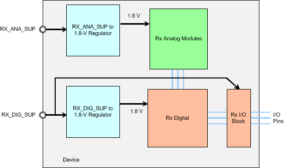
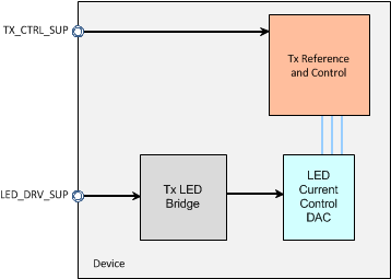
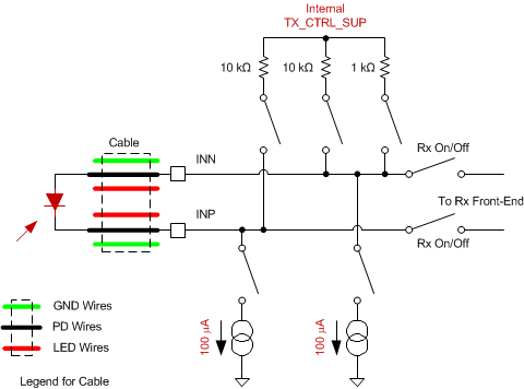
8.3.4 Receiver Subsystem Power Path
The block diagram in Figure 65 shows the device Rx subsystem power routing.
8.3.5 Transmit Section
The transmit section integrates the LED driver and the LED current control section with 8-bit resolution. This integration is designed to meet a dynamic range of better than 105 dB (based on a 1-sigma LED current noise).
The RED and IR LED reference currents can be independently set. The current source (ILED) locally regulates and ensures that the actual LED current tracks the specified reference. The transmitter section uses a reference voltage for operation. This reference voltage is available on the REF_TX pin and must be decoupled to ground with a 2.2-μF capacitor. The TX_REF voltage is derived from the TX_CTRL_SUP. The maximum LED current setting depends on the transmitter reference voltage. By default, after reset, this voltage is 0.75 V and supports up to a 150-mA LED current. For higher LED currents up to 200 mA, the reference can be programmed to 1.0 V (using the LED_RANGE[1:0] register bits).
The minimum LED_DRV_SUP voltage required for operation depends on the:
- Voltage drop across the LED (VLED),
- Voltage drop across the external cable, connector, and any other component in series with the LED (VCABLE), and
- Transmitter reference voltage.
Using the default reference voltage of 0.75 V, the minimum LED_DRV_SUP voltage can be as low as 3.25 V, provided that Equation 3 is met. Refer to the Recommended Operating Conditions table.
To lower the minimum LED_DRV_SUP voltage even further, the transmitter reference voltage can be programmed to 0.5 V. By doing so, the minimum LED_DRV_SUP voltage can be reduced to 3.0 V, provided that Equation 4 is met. Refer to the Recommended Operating Conditions table.
Note that with the 0.5-V transmitter reference voltage, the maximum LED current supported is 100 mA.
Two LED driver schemes are supported:
- An H-bridge drive for a two-pin, back-to-back LED package, as shown in Figure 66.
- A push-pull drive for a three-pin, common-anode LED package; see Figure 67.
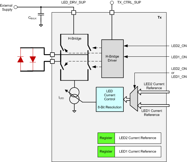 Figure 66. Transmit: H-Bridge Drive
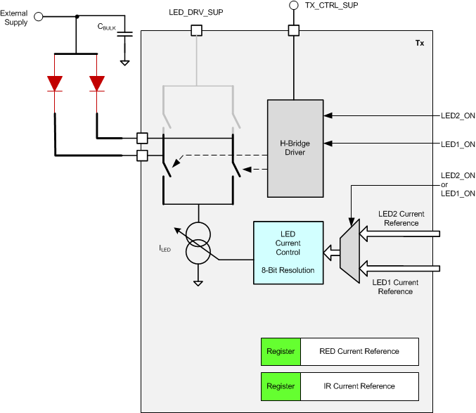 Figure 67. Transmit: Push-Pull LED Drive for Common Anode LED Configuration
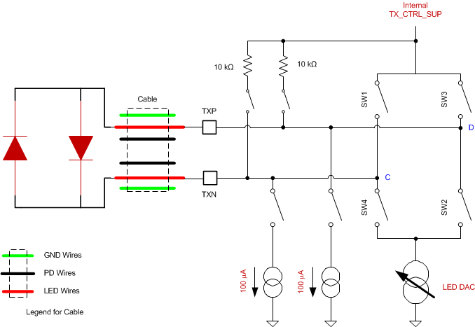
8.3.5.1 Transmitter Power Path
The block diagram in Figure 68 shows the device Tx subsystem power routing.
8.3.5.2 LED Power Reduction During Periods of Inactivity
The diagram in Figure 69 shows how LED bias current passes 50 µA whenever LED_ON occurs. In order to minimize power consumption in periods of inactivity, the LED_ON control must be turned off. Furthermore, disable the TIMEREN bit in the CONTROL1 register by setting the value to '0'.
Note that depending on the LEDs used, the LED may sometimes appear dimly lit even when the LED current is set to 0 mA. This appearance is because of the switching leakage currents (as shown in Figure 69) inherent to the timer function. The dimmed appearance does not effect the ambient light level measurement because during the ambient cycle, LED_ON is turned off for the duration of the ambient measurement.
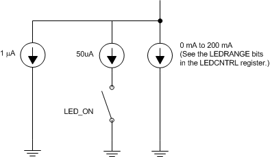 Figure 69. LED Bias Current
8.4 Device Functional Modes
8.4.1 ADC Operation and Averaging Module
After the falling edge of the ADC reset signal, the ADC conversion phase starts (refer to Figure 64). Each ADC conversion takes 50 µs.
There are two modes of operation: without averaging and with averaging. The averaging mode can average multiple ADC samples and reduce noise to improve dynamic range because the ADC conversion time is usually shorter than 25% of the pulse repetition period. Figure 70 shows a diagram of the averaging module. The ADC output format is in 22-bit twos complement. The two MSB bits of the 24-bit data can be ignored.
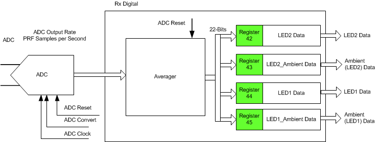 Figure 70. Averaging Module
8.4.1.1 Operation Without Averaging
In this mode, the ADC outputs a digital sample one time for every 50 µs. At the next rising edge of the ADC reset signal, the first 22-bit conversion value is written into the result registers sequentially as follows (see Figure 71):
- At the 25% reset signal, the first 22-bit ADC sample is written to register 2Ah.
- At the 50% reset signal, the first 22-bit ADC sample is written to register 2Bh.
- At the 75% reset signal, the first 22-bit ADC sample is written to register 2Ch.
- At the next 0% reset signal, the first 22-bit ADC sample is written to register 2Dh. The contents of registers 2Ah and 2Bh are written to register 2Eh and the contents of registers 2Ch and 2Dh are written to register 2Fh.
At the rising edge of the ADC_RDY signal, the contents of all six result registers can be read out.
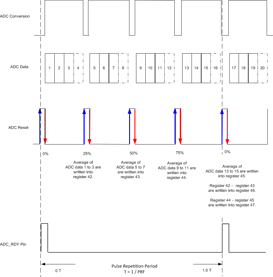
8.4.1.2 Operation With Averaging
In this mode, all ADC digital samples are accumulated and averaged after every 50 µs. At the next rising edge of the ADC reset signal, the average value (22-bit) is written into the output registers sequentially as follows (see Figure 72):
- At the 25% reset signal, the averaged 22-bit word is written to register 2Ah.
- At the 50% reset signal, the averaged 22-bit word is written to register 2Bh.
- At the 75% reset signal, the averaged 22-bit word is written to register 2Ch.
- At the next 0% reset signal, the averaged 22-bit word is written to register 2Dh. The contents of registers 2Ah and 2Bh are written to register 2Eh and the contents of registers 2Ch and 2Dh are written to register 2Fh.
At the rising edge of the ADC_RDY signal, the contents of all six result registers can be read out.
The number of samples to be used per conversion phase is specified in the CONTROL1 register (NUMAV[7:0]). The user must specify the correct value for the number of averages, as described in Equation 5:
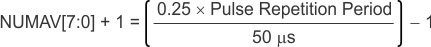
When the number of averages is '0', the averaging is disabled and only one ADC sample is written to the result registers.
Note that he number of average conversions is limited by 25% of the PRF. For example, eight samples can be averaged with PRF = 625 Hz, and four samples can be averaged with PRF = 1250 Hz.
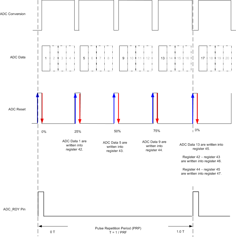 Figure 71. ADC Data without Averaging (when Number of Averages = 0)
8.4.2 AFE Analog Output Mode (ADC Bypass Mode)
This mode is only intended for use in system debug. Note that this function is not recommended for production use because of the minimal device production testing performed on this function.
The ADC bypass mode brings out the analog output voltage of the receiver front-end on two pins (RXOUTP, RXOUTN), around a common-mode voltage of approximately 0.9 V. In this mode, the internal ADC of the AFE4490 is disabled. Figure 73 shows a block diagram of this mode.
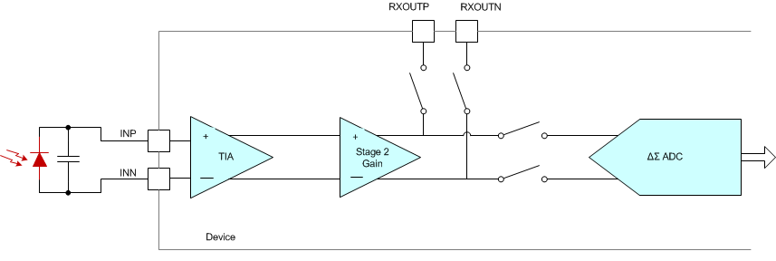 Figure 73. Device Set to ADC Bypass Mode
In ADC bypass mode, one of the internal clocks (ADC_Reset) can be brought out on the PD_ALM pin, as shown in Figure 74. This signal can be used to convert each of the four phases (within every pulse repetition period). Additionally, the ADC_RDY signal can be used to synchronize the external ADC with the AFE. See Figure 75 for the timing of this mode.
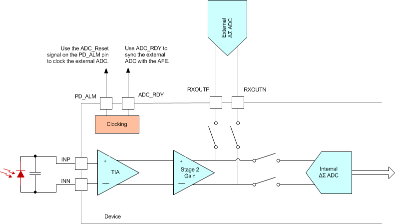 Figure 74. Device in ADC Bypass Mode with ADC_Reset to PD_ALM Pin
In ADC bypass mode, the ADC reset signal can be used to start conversions with the external ADC. Use registers 15h through 1Ch to position the ADC reset signal edges appropriately. Also, use the CLKALMPIN[2:0] bits on the PD_ALM pin register bit to bring out the ADC reset signal to the PD_ALM pin. ADC_RDY can be used to indicate the start of the pulse repetition period to the external ADC.
8.4.3 Diagnostics
The device includes diagnostics to detect open or short conditions of the LED and photosensor, LED current profile feedback, and cable on or off detection.
8.4.3.1 Photodiode-Side Fault Detection
Figure 76 shows the diagnostic for the photodiode-side fault detection.
8.4.3.2 Transmitter-Side Fault Detection
Figure 77 shows the diagnostic for the transmitter-side fault detection.
8.4.3.3 Diagnostics Module
The diagnostics module, when enabled, checks for nine types of faults sequentially. The results of all faults are latched in 11 separate flags. At the end of the sequence, the state of the 11 flags are combined to generate two interrupt signals: PD_ALM for photodiode-related faults and LED_ALM for transmit-related faults. The status of all flags can also be read using the SPI interface. Table 3 details each fault and flag used. Note that the diagnostics module requires all AFE blocks to be enabled in order to function reliably.
Table 3. Fault and Flag Diagnostics(1)
Figure 78 shows the timing for the diagnostic function.
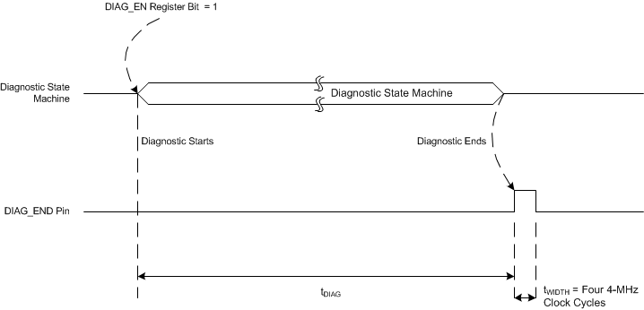 Figure 78. Diagnostic Timing Diagram
By default, the diagnostic function takes tDIAG = 8 ms to complete after the DIAG_EN register bit is enabled. By setting the EN_SLOW_DIAG register bit (CONTROL2 register, bit D8) the diagnostic time can be increased to
16 ms.
After completion of the diagnostics function, time must be allowed for the device filter to settle. See the Electrical Characteristics for the filter settling time. The slow diagnostics feature is provided for use in systems where high-capacitance sensors (such as photodiodes, capacitors, cables, and so forth) are connected to the INP, INN, TXP, or TXN pins.
8.5 Programming
8.5.1 Serial Programming Interface
The SPI-compatible serial interface consists of four signals: SCLK (serial clock), SPISOMI (serial interface data output), SPISIMO (serial interface data input), and SPISTE (serial interface enable).
The serial clock (SCLK) is the serial peripheral interface (SPI) serial clock. SCLK shifts in commands and shifts out data from the device. SCLK features a Schmitt-triggered input and clocks data out on SPISOMI. Data are clocked in on the SPISIMO pin. Even though the input has hysteresis, TI recommends keeping SCLK as clean as possible to prevent glitches from accidentally shifting the data. When the serial interface is idle, hold SCLK low.
The SPISOMI (SPI serial out master in) pin is used with SCLK to clock out device data. The SPISIMO (SPI serial in master out) pin is used with SCLK to clock in data to the device. The SPISTE (SPI serial interface enable) pin enables the serial interface to clock data on the SPISIMO pin in to the device.
8.5.2 Reading and Writing Data
The device has a set of internal registers that can be accessed by the serial programming interface formed by the SPISTE, SCLK, SPISIMO, and SPISOMI pins.
8.5.2.1 Writing Data
The SPI_READ register bit must be first set to '0' before writing to a register. When SPISTE is low,
- Serially shifting bits into the device is enabled.
- Serial data (on the SPISIMO pin) are latched at every SCLK rising edge.
- The serial data are loaded into the register at every 32nd SCLK rising edge.
In case the word length exceeds a multiple of 32 bits, the excess bits are ignored. Data can be loaded in multiples of 32-bit words within a single active SPISTE pulse. The first eight bits form the register address and the remaining 24 bits form the register data. Figure 79 shows an SPI timing diagram for a single write operation. For multiple read and write cycles, refer to the Multiple Data Reads and Writes section.
 Figure 79. AFE SPI Write Timing Diagram
8.5.2.2 Reading Data
The SPI_READ register bit must be first set to '1' before reading from a register. The device includes a mode where the contents of the internal registers can be read back on the SPISOMI pin. This mode may be useful as a diagnostic check to verify the serial interface communication between the external controller and the AFE. To enable this mode, first set the SPI_READ register bit using the SPI write command, as described in the Writing Data section. In the next command, specify the SPI register address with the desired content to be read. Within the same SPI command sequence, the AFE outputs the contents of the specified register on the SPISOMI pin. Figure 80 shows an SPI timing diagram for a single read operation. For multiple read and write cycles, refer to the Multiple Data Reads and Writes section.
8.5.2.3 Multiple Data Reads and Writes
The device includes functionality where multiple read and write operations can be performed during a single SPISTE event. To enable this functionality, the first eight bits determine the register address to be written and the remaining 24 bits determine the register data. Perform two writes with the SPI read bit enabled during the second write operation in order to prepare for the read operation, as described in the Writing Data section. In the next command, specify the SPI register address with the desired content to be read. Within the same SPI command sequence, the AFE outputs the contents of the specified register on the SPISOMI pin. This functionality is described in the Writing Data and Reading Data sections. Figure 81 shows a timing diagram for the SPI multiple read and write operations.
8.5.2.4 Register Initialization
After power-up, the internal registers must be initialized to the default values. This initialization can be done in one of two ways:
- Through a hardware reset by applying a low-going pulse on the RESET pin, or
- By applying a software reset. Using the serial interface, set SW_RESET (bit D3 in register 00h) high. This setting initializes the internal registers to the default values and then self-resets to '0'. In this case, the RESET pin is kept high (inactive).
8.5.2.5 AFE SPI Interface Design Considerations
Note that when the device is deselected, the SPISOMI, CLKOUT, ADC_RDY, PD_ALM, LED_ALM, and DIAG_END digital output pins do not enter a 3-state mode. This condition, therefore, must be taken into account when connecting multiple devices to the SPI port and for power-management considerations. In order to avoid loading the SPI bus when multiple devices are connected, the DIGOUT_TRISTATE register bit must be to '1' whenever the AFE SPI is inactive.
8.6 Register Maps
The AFE consists of a set of registers that can be used to configure it, such as receiver timings, I-V amplifier settings, transmit LED currents, and so forth. The registers and their contents are listed in Table 4. These registers can be accessed using the AFE SPI interface.
Table 4. AFE Register Map
| NAME | REGISTER CONTROL(1) | ADDRESS | REGISTER DATA | ||||||||||||||||||||||||
|---|---|---|---|---|---|---|---|---|---|---|---|---|---|---|---|---|---|---|---|---|---|---|---|---|---|---|---|
| Hex | Dec | D23 | D22 | D21 | D20 | D19 | D18 | D17 | D16 | D15 | D14 | D13 | D12 | D11 | D10 | D9 | D8 | D7 | D6 | D5 | D4 | D3 | D2 | D1 | D0 | ||
| CONTROL0 | W | 00 | 0 | 0 | 0 | 0 | 0 | 0 | 0 | 0 | 0 | 0 | 0 | 0 | 0 | 0 | 0 | 0 | 0 | 0 | 0 | 0 | 0 | SW_RST | DIAG_EN | TIM_COUNT_RST | SPI_READ |
| LED2STC | R/W | 01 | 1 | 0 | 0 | 0 | 0 | 0 | 0 | 0 | 0 | LED2STC[15:0] | |||||||||||||||
| LED2ENDC | R/W | 02 | 2 | 0 | 0 | 0 | 0 | 0 | 0 | 0 | 0 | LED2ENDC[15:0] | |||||||||||||||
| LED2LEDSTC | R/W | 03 | 3 | 0 | 0 | 0 | 0 | 0 | 0 | 0 | 0 | LED2LEDSTC[15:0] | |||||||||||||||
| LED2LEDENDC | R/W | 04 | 4 | 0 | 0 | 0 | 0 | 0 | 0 | 0 | 0 | LED2LEDENDC[15:0] | |||||||||||||||
| ALED2STC | R/W | 05 | 5 | 0 | 0 | 0 | 0 | 0 | 0 | 0 | 0 | ALED2STC[15:0] | |||||||||||||||
| ALED2ENDC | R/W | 06 | 6 | 0 | 0 | 0 | 0 | 0 | 0 | 0 | 0 | ALED2ENDC[15:0] | |||||||||||||||
| LED1STC | R/W | 07 | 7 | 0 | 0 | 0 | 0 | 0 | 0 | 0 | 0 | LED1STC[15:0] | |||||||||||||||
| LED1ENDC | R/W | 08 | 8 | 0 | 0 | 0 | 0 | 0 | 0 | 0 | 0 | LED1ENDC[15:0] | |||||||||||||||
| LED1LEDSTC | R/W | 09 | 9 | 0 | 0 | 0 | 0 | 0 | 0 | 0 | 0 | LED1LEDSTC[15:0] | |||||||||||||||
| LED1LEDENDC | R/W | 0A | 10 | 0 | 0 | 0 | 0 | 0 | 0 | 0 | 0 | LED1LEDENDC[15:0] | |||||||||||||||
| ALED1STC | R/W | 0B | 11 | 0 | 0 | 0 | 0 | 0 | 0 | 0 | 0 | ALED1STC[15:0] | |||||||||||||||
| ALED1ENDC | R/W | 0C | 12 | 0 | 0 | 0 | 0 | 0 | 0 | 0 | 0 | ALED1ENDC[15:0] | |||||||||||||||
| LED2CONVST | R/W | 0D | 13 | 0 | 0 | 0 | 0 | 0 | 0 | 0 | 0 | LED2CONVST[15:0] | |||||||||||||||
| LED2CONVEND | R/W | 0E | 14 | 0 | 0 | 0 | 0 | 0 | 0 | 0 | 0 | LED2CONVEND[15:0] | |||||||||||||||
| ALED2CONVST | R/W | 0F | 15 | 0 | 0 | 0 | 0 | 0 | 0 | 0 | 0 | ALED2CONVST[15:0] | |||||||||||||||
| ALED2CONVEND | R/W | 10 | 16 | 0 | 0 | 0 | 0 | 0 | 0 | 0 | 0 | ALED2CONVEND[15:0] | |||||||||||||||
| LED1CONVST | R/W | 11 | 17 | 0 | 0 | 0 | 0 | 0 | 0 | 0 | 0 | LED1CONVST[15:0] | |||||||||||||||
| LED1CONVEND | R/W | 12 | 18 | 0 | 0 | 0 | 0 | 0 | 0 | 0 | 0 | LED1CONVEND[15:0] | |||||||||||||||
| ALED1CONVST | R/W | 13 | 19 | 0 | 0 | 0 | 0 | 0 | 0 | 0 | 0 | ALED1CONVST[15:0] | |||||||||||||||
| ALED1CONVEND | R/W | 14 | 20 | 0 | 0 | 0 | 0 | 0 | 0 | 0 | 0 | ALED1CONVEND[15:0] | |||||||||||||||
| ADCRSTSTCT0 | R/W | 15 | 21 | 0 | 0 | 0 | 0 | 0 | 0 | 0 | 0 | ADCRSTCT0[15:0] | |||||||||||||||
| ADCRSTENDCT0 | R/W | 16 | 22 | 0 | 0 | 0 | 0 | 0 | 0 | 0 | 0 | ADCRENDCT0[15:0] | |||||||||||||||
| ADCRSTSTCT1 | R/W | 17 | 23 | 0 | 0 | 0 | 0 | 0 | 0 | 0 | 0 | ADCRSTCT1[15:0] | |||||||||||||||
| ADCRSTENDCT1 | R/W | 18 | 24 | 0 | 0 | 0 | 0 | 0 | 0 | 0 | 0 | ADCRENDCT1[15:0] | |||||||||||||||
| ADCRSTSTCT2 | R/W | 19 | 25 | 0 | 0 | 0 | 0 | 0 | 0 | 0 | 0 | ADCRSTCT2[15:0] | |||||||||||||||
| ADCRSTENDCT2 | R/W | 1A | 26 | 0 | 0 | 0 | 0 | 0 | 0 | 0 | 0 | ADCRENDCT2[15:0] | |||||||||||||||
| ADCRSTSTCT3 | R/W | 1B | 27 | 0 | 0 | 0 | 0 | 0 | 0 | 0 | 0 | ADCRSTCT3[15:0] | |||||||||||||||
| ADCRSTENDCT3 | R/W | 1C | 28 | 0 | 0 | 0 | 0 | 0 | 0 | 0 | 0 | ADCRENDCT3[15:0] | |||||||||||||||
| PRPCOUNT | R/W | 1D | 29 | 0 | 0 | 0 | 0 | 0 | 0 | 0 | 0 | PRPCT[15:0] | |||||||||||||||
| CONTROL1 | R/W | 1E | 30 | 0 | 0 | 0 | 0 | 0 | 0 | 0 | 0 | 0 | 0 | 0 | 0 | CLKALMPIN[2:0] | TIMEREN | NUMAV[7:0] | |||||||||
| SPARE1 | N/A | 1F | 31 | 0 | 0 | 0 | 0 | 0 | 0 | 0 | 0 | 0 | 0 | 0 | 0 | 0 | 0 | 0 | 0 | 0 | 0 | 0 | 0 | 0 | 0 | 0 | 0 |
| TIAGAIN | R/W | 20 | 32 | 0 | 0 | 0 | 0 | 0 | 0 | 0 | 0 | ENSEPGAN | STAGE2EN1 | 0 | 0 | 0 | STG2GAIN1[2:0] | CF_LED1[4:0] | RF_LED1[2:0] | ||||||||
| TIA_AMB_GAIN | R/W | 21 | 33 | 0 | 0 | 0 | 0 | AMBDAC[3:0] | FLTRCNRSEL | STAGE2EN2 | 0 | 0 | 0 | STG2GAIN2[2:0] | CF_LED2[4:0] | RF_LED2[2:0] | |||||||||||
| LEDCNTRL | R/W | 22 | 34 | 0 | 0 | 0 | 0 | 0 | 0 | LED RANGE[1:0] |
LED1[7:0] | LED2[7:0] | |||||||||||||||
| CONTROL2 | R/W | 23 | 35 | 0 | 0 | 0 | 0 | 0 | TX_REF1 | TX_REF0 | RST_CLK_ON_PD_ALM | EN_ADC_BYP | 0 | 0 | 0 | TXBRGMOD | DIGOUT_TRISTATE | XTALDIS | EN_SLOW_DIAG | 0 | 0 | 0 | 0 | 0 | PDNTX | PDNRX | PDNAFE |
| SPARE2 | N/A | 24 | 36 | 0 | 0 | 0 | 0 | 0 | 0 | 0 | 0 | 0 | 0 | 0 | 0 | 0 | 0 | 0 | 0 | 0 | 0 | 0 | 0 | 0 | 0 | 0 | 0 |
| SPARE3 | N/A | 25 | 37 | 0 | 0 | 0 | 0 | 0 | 0 | 0 | 0 | 0 | 0 | 0 | 0 | 0 | 0 | 0 | 0 | 0 | 0 | 0 | 0 | 0 | 0 | 0 | 0 |
| SPARE4 | N/A | 26 | 38 | 0 | 0 | 0 | 0 | 0 | 0 | 0 | 0 | 0 | 0 | 0 | 0 | 0 | 0 | 0 | 0 | 0 | 0 | 0 | 0 | 0 | 0 | 0 | 0 |
| RESERVED1 | N/A | 27 | 39 | X | X | X | X | X | X | X | X | X | X | X | X | X | X | X | X | X | X | X | X | X | X | X | X |
| RESERVED2 | N/A | 28 | 40 | X | X | X | X | X | X | X | X | X | X | X | X | X | X | X | X | X | X | X | X | X | X | X | X |
| ALARM | R/W | 29 | 41 | 0 | 0 | 0 | 0 | 0 | 0 | 0 | 0 | 0 | 0 | 0 | 0 | 0 | 0 | 0 | 0 | ALMPINCLKEN | 0 | 0 | 0 | 0 | 0 | 0 | 0 |
| LED2VAL | R | 2A | 42 | LED2VAL[23:0] | |||||||||||||||||||||||
| ALED2VAL | R | 2B | 43 | ALED2VAL[23:0] | |||||||||||||||||||||||
| LED1VAL | R | 2C | 44 | LED1VAL[23:0] | |||||||||||||||||||||||
| ALED1VAL | R | 2D | 45 | ALED1VAL[23:0] | |||||||||||||||||||||||
| LED2-ALED2VAL | R | 2E | 46 | LED2-ALED2VAL[23:0] | |||||||||||||||||||||||
| LED1-ALED1VAL | R | 2F | 47 | LED1-ALED1VAL[23:0] | |||||||||||||||||||||||
| DIAG | R | 30 | 48 | 0 | 0 | 0 | 0 | 0 | 0 | 0 | 0 | 0 | 0 | 0 | PD_ALM | LED_ALM | LED1OPEN | LED2OPEN | LEDSC | OUTPSHGN | OUTNSHGND | PDOC | PDSC | INNSCGND | INPSCGND | INNSCLED | INPSCLED |
8.6.1 AFE Register Description
| D23 | D22 | D21 | D20 | D19 | D18 | D17 | D16 | D15 | D14 | D13 | D12 |
| 0 | 0 | 0 | 0 | 0 | 0 | 0 | 0 | 0 | 0 | 0 | 0 |
| W-0h | W-0h | W-0h | W-0h | W-0h | W-0h | W-0h | W-0h | W-0h | W-0h | W-0h | W-0h |
| D11 | D10 | D9 | D8 | D7 | D6 | D5 | D4 | D3 | D2 | D1 | D0 |
| 0 | 0 | 0 | 0 | 0 | 0 | 0 | 0 | SW_RST | DIAG_EN | TIM_ COUNT_ RST |
SPI_ READ |
| W-0h | W-0h | W-0h | W-0h | W-0h | W-0h | W-0h | W-0h | W-0h | W-0h | W-0h | W-0h |
| LEGEND: W = Write only; -n = value after reset |
This register is write-only. CONTROL0 is used for AFE software and count timer reset, diagnostics enable, and SPI read functions.
| Bits D[23:4] | Must be '0' |
| Bit D3 | SW_RST: Software reset |
| 0 = No action (default after reset) 1 = Software reset applied; resets all internal registers to the default values and self-clears to '0' |
|
| Bit D2 | DIAG_EN: Diagnostic enable |
| 0 = No Action (default after reset) 1 = Diagnostic mode is enabled and the diagnostics sequence starts when this bit is set. At the end of the sequence, all fault statuses are stored in the DIAG: Diagnostics Flag Register. Afterwards, the DIAG_EN register bit self-clears to '0'. Note that the diagnostics enable bit is automatically reset after the diagnostics completes (slow =16 ms, fast = 8 ms). During diagnostics mode, the ADC data are invalid because of toggling diagnostics switches. |
|
| Bit D1 | TIM_CNT_RST: Timer counter reset |
| 0 = Disables timer counter reset, required for normal timer operation (default after reset) 1 = Timer counters are in reset state |
|
| Bit D0 | SPI READ: SPI read |
| 0 = SPI read is disabled (default after reset) 1 = SPI read is enabled |
| D23 | D22 | D21 | D20 | D19 | D18 | D17 | D16 | D15 | D14 | D13 | D12 |
| 0 | 0 | 0 | 0 | 0 | 0 | 0 | 0 | LED2STC[15:0] | |||
| R/W-0h | R/W-0h | R/W-0h | R/W-0h | R/W-0h | R/W-0h | R/W-0h | R/W-0h | R/W-0h | |||
| D11 | D10 | D9 | D8 | D7 | D6 | D5 | D4 | D3 | D2 | D1 | D0 |
| LED2STC[15:0] | |||||||||||
| R/W-0h | |||||||||||
| LEGEND: R/W = Read/Write; -n = value after reset |
This register sets the start timing value for the LED2 signal sample.
| Bits D[23:16] | Must be '0' |
| Bits D[15:0] | LED2STC[15:0]: Sample LED2 start count |
| The contents of this register can be used to position the start of the sample LED2 signal with respect to the pulse repetition period (PRP), as specified in the PRPCOUNT register. The count is specified as the number of 4-MHz clock cycles. Refer to the Using the Timer Module section for details. |
| D23 | D22 | D21 | D20 | D19 | D18 | D17 | D16 | D15 | D14 | D13 | D12 |
| 0 | 0 | 0 | 0 | 0 | 0 | 0 | 0 | LED2ENDC[15:0] | |||
| R/W-0h | R/W-0h | R/W-0h | R/W-0h | R/W-0h | R/W-0h | R/W-0h | R/W-0h | R/W-0h | |||
| D11 | D10 | D9 | D8 | D7 | D6 | D5 | D4 | D3 | D2 | D1 | D0 |
| LED2ENDC[15:0] | |||||||||||
| R/W-0h | |||||||||||
| LEGEND: R/W = Read/Write; -n = value after reset |
This register sets the end timing value for the LED2 signal sample.
| Bits D[23:16] | Must be '0' |
| Bits D[15:0] | LED2ENDC[15:0]: Sample LED2 end count |
| The contents of this register can be used to position the end of the sample LED2 signal with respect to the PRP, as specified in the PRPCOUNT register. The count is specified as the number of 4-MHz clock cycles. Refer to the Using the Timer Module section for details. |
| D23 | D22 | D21 | D20 | D19 | D18 | D17 | D16 | D15 | D14 | D13 | D12 |
| 0 | 0 | 0 | 0 | 0 | 0 | 0 | 0 | LED2LEDSTC[15:0] | |||
| R/W-0h | R/W-0h | R/W-0h | R/W-0h | R/W-0h | R/W-0h | R/W-0h | R/W-0h | R/W-0h | |||
| D11 | D10 | D9 | D8 | D7 | D6 | D5 | D4 | D3 | D2 | D1 | D0 |
| LED2LEDSTC[15:0] | |||||||||||
| R/W-0h | |||||||||||
| LEGEND: R/W = Read/Write; -n = value after reset |
This register sets the start timing value for when the LED2 signal turns on.
| Bits D[23:16] | Must be '0' |
| Bits D[15:0] | LED2LEDSTC[15:0]: LED2 start count |
| The contents of this register can be used to position the start of the LED2 with respect to the PRP, as specified in the PRPCOUNT register. The count is specified as the number of 4-MHz clock cycles. Refer to the Using the Timer Module section for details. |
| D23 | D22 | D21 | D20 | D19 | D18 | D17 | D16 | D15 | D14 | D13 | D12 |
| 0 | 0 | 0 | 0 | 0 | 0 | 0 | 0 | LED2LEDENDC[15:0] | |||
| R/W-0h | R/W-0h | R/W-0h | R/W-0h | R/W-0h | R/W-0h | R/W-0h | R/W-0h | R/W-0h | |||
| D11 | D10 | D9 | D8 | D7 | D6 | D5 | D4 | D3 | D2 | D1 | D0 |
| LED2LEDENDC[15:0] | |||||||||||
| R/W-0h | |||||||||||
| LEGEND: R/W = Read/Write; -n = value after reset |
This register sets the end timing value for when the LED2 signal turns off.
| Bits D[23:16] | Must be '0' |
| Bits D[15:0] | LED2LEDENDC[15:0]: LED2 end count |
| The contents of this register can be used to position the end of the LED2 signal with respect to the PRP, as specified in the PRPCOUNT register. The count is specified as the number of 4-MHz clock cycles. Refer to the Using the Timer Module section for details. |
| D23 | D22 | D21 | D20 | D19 | D18 | D17 | D16 | D15 | D14 | D13 | D12 |
| 0 | 0 | 0 | 0 | 0 | 0 | 0 | 0 | ALED2STC[15:0] | |||
| R/W-0h | R/W-0h | R/W-0h | R/W-0h | R/W-0h | R/W-0h | R/W-0h | R/W-0h | R/W-0h | |||
| D11 | D10 | D9 | D8 | D7 | D6 | D5 | D4 | D3 | D2 | D1 | D0 |
| ALED2STC[15:0] | |||||||||||
| R/W-0h | |||||||||||
| LEGEND: R/W = Read/Write; -n = value after reset |
This register sets the start timing value for the ambient LED2 signal sample.
| Bits D[23:16] | Must be '0' |
| Bits D[15:0] | ALED2STC[15:0]: Sample ambient LED2 start count |
| The contents of this register can be used to position the start of the sample ambient LED2 signal with respect to the PRP, as specified in the PRPCOUNT register. The count is specified as the number of 4-MHz clock cycles. Refer to the Using the Timer Module section for details. |
(Address = 06h, Reset Value = 0000h)
| D23 | D22 | D21 | D20 | D19 | D18 | D17 | D16 | D15 | D14 | D13 | D12 |
| 0 | 0 | 0 | 0 | 0 | 0 | 0 | 0 | ALED2ENDC[15:0] | |||
| R/W-0h | R/W-0h | R/W-0h | R/W-0h | R/W-0h | R/W-0h | R/W-0h | R/W-0h | R/W-0h | |||
| D11 | D10 | D9 | D8 | D7 | D6 | D5 | D4 | D3 | D2 | D1 | D0 |
| ALED2ENDC[15:0] | |||||||||||
| R/W-0h | |||||||||||
| LEGEND: R/W = Read/Write; -n = value after reset |
This register sets the end timing value for the ambient LED2 signal sample.
| Bits D[23:16] | Must be '0' |
| Bits D[15:0] | ALED2ENDC[15:0]: Sample ambient LED2 end count |
| The contents of this register can be used to position the end of the sample ambient LED2 signal with respect to the PRP, as specified in the PRPCOUNT register. The count is specified as the number of 4-MHz clock cycles. Refer to the Using the Timer Module section for details. |
| D23 | D22 | D21 | D20 | D19 | D18 | D17 | D16 | D15 | D14 | D13 | D12 |
| 0 | 0 | 0 | 0 | 0 | 0 | 0 | 0 | LED1STC[15:0] | |||
| R/W-0h | R/W-0h | R/W-0h | R/W-0h | R/W-0h | R/W-0h | R/W-0h | R/W-0h | R/W-0h | |||
| D11 | D10 | D9 | D8 | D7 | D6 | D5 | D4 | D3 | D2 | D1 | D0 |
| LED1STC[15:0] | |||||||||||
| R/W-0h | |||||||||||
| LEGEND: R/W = Read/Write; -n = value after reset |
This register sets the start timing value for the LED1 signal sample.
| Bits D[23:17] | Must be '0' |
| Bits D[16:0] | LED1STC[15:0]: Sample LED1 start count |
| The contents of this register can be used to position the start of the sample LED1 signal with respect to the PRP, as specified in the PRPCOUNT register. The count is specified as the number of 4-MHz clock cycles. Refer to the Using the Timer Module section for details. |
| D23 | D22 | D21 | D20 | D19 | D18 | D17 | D16 | D15 | D14 | D13 | D12 |
| 0 | 0 | 0 | 0 | 0 | 0 | 0 | 0 | LED1ENDC[15:0] | |||
| R/W-0h | R/W-0h | R/W-0h | R/W-0h | R/W-0h | R/W-0h | R/W-0h | R/W-0h | R/W-0h | |||
| D11 | D10 | D9 | D8 | D7 | D6 | D5 | D4 | D3 | D2 | D1 | D0 |
| LED1ENDC[15:0] | |||||||||||
| R/W-0h | |||||||||||
| LEGEND: R/W = Read/Write; -n = value after reset |
This register sets the end timing value for the LED1 signal sample.
| Bits D[23:17] | Must be '0' |
| Bits D[16:0] | LED1ENDC[15:0]: Sample LED1 end count |
| The contents of this register can be used to position the end of the sample LED1 signal with respect to the PRP, as specified in the PRPCOUNT register. The count is specified as the number of 4-MHz clock cycles. Refer to the Using the Timer Module section for details. |
| D23 | D22 | D21 | D20 | D19 | D18 | D17 | D16 | D15 | D14 | D13 | D12 |
| 0 | 0 | 0 | 0 | 0 | 0 | 0 | 0 | LED1LEDSTC[15:0] | |||
| R/W-0h | R/W-0h | R/W-0h | R/W-0h | R/W-0h | R/W-0h | R/W-0h | R/W-0h | R/W-0h | |||
| D11 | D10 | D9 | D8 | D7 | D6 | D5 | D4 | D3 | D2 | D1 | D0 |
| LED1LEDSTC[15:0] | |||||||||||
| R/W-0h | |||||||||||
| LEGEND: R/W = Read/Write; -n = value after reset |
This register sets the start timing value for when the LED1 signal turns on.
| Bits D[23:16] | Must be '0' |
| Bits D[15:0] | LED1LEDSTC[15:0]: LED1 start count |
| The contents of this register can be used to position the start of the LED1 signal with respect to the PRP, as specified in the PRPCOUNT register. The count is specified as the number of 4-MHz clock cycles. Refer to the Using the Timer Module section for details. |
| D23 | D22 | D21 | D20 | D19 | D18 | D17 | D16 | D15 | D14 | D13 | D12 |
| 0 | 0 | 0 | 0 | 0 | 0 | 0 | 0 | LED1LEDENDC[15:0] | |||
| R/W-0h | R/W-0h | R/W-0h | R/W-0h | R/W-0h | R/W-0h | R/W-0h | R/W-0h | R/W-0h | |||
| D11 | D10 | D9 | D8 | D7 | D6 | D5 | D4 | D3 | D2 | D1 | D0 |
| LED1LEDENDC[15:0] | |||||||||||
| R/W-0h | |||||||||||
| LEGEND: R/W = Read/Write; -n = value after reset |
This register sets the end timing value for when the LED1 signal turns off.
| Bits D[23:16] | Must be '0' |
| Bits D[15:0] | LED1LEDENDC[15:0]: LED1 end count |
| The contents of this register can be used to position the end of the LED1 signal with respect to the PRP, as specified in the PRPCOUNT register. The count is specified as the number of 4-MHz clock cycles. Refer to the Using the Timer Module section for details. |
| D23 | D22 | D21 | D20 | D19 | D18 | D17 | D16 | D15 | D14 | D13 | D12 |
| 0 | 0 | 0 | 0 | 0 | 0 | 0 | 0 | ALED1STC[15:0] | |||
| R/W-0h | R/W-0h | R/W-0h | R/W-0h | R/W-0h | R/W-0h | R/W-0h | R/W-0h | R/W-0h | |||
| D11 | D10 | D9 | D8 | D7 | D6 | D5 | D4 | D3 | D2 | D1 | D0 |
| ALED1STC[15:0] | |||||||||||
| R/W-0h | |||||||||||
| LEGEND: R/W = Read/Write; -n = value after reset |
This register sets the start timing value for the ambient LED1 signal sample.
| Bits D[23:16] | Must be '0' |
| Bits D[15:0] | ALED1STC[15:0]: Sample ambient LED1 start count |
| The contents of this register can be used to position the start of the sample ambient LED1 signal with respect to the PRP, as specified in the PRPCOUNT register. The count is specified as the number of 4-MHz clock cycles. Refer to the Using the Timer Module section for details. |
(Address = 0Ch, Reset Value = 0000h)
| D23 | D22 | D21 | D20 | D19 | D18 | D17 | D16 | D15 | D14 | D13 | D12 |
| 0 | 0 | 0 | 0 | 0 | 0 | 0 | 0 | ALED1ENDC[15:0] | |||
| R/W-0h | R/W-0h | R/W-0h | R/W-0h | R/W-0h | R/W-0h | R/W-0h | R/W-0h | R/W-0h | |||
| D11 | D10 | D9 | D8 | D7 | D6 | D5 | D4 | D3 | D2 | D1 | D0 |
| ALED1ENDC[15:0] | |||||||||||
| R/W-0h | |||||||||||
| LEGEND: R/W = Read/Write; -n = value after reset |
This register sets the end timing value for the ambient LED1 signal sample.
| Bits D[23:16] | Must be '0' |
| Bits D[15:0] | ALED1ENDC[15:0]: Sample ambient LED1 end count |
| The contents of this register can be used to position the end of the sample ambient LED1 signal with respect to the PRP, as specified in the PRPCOUNT register. The count is specified as the number of 4-MHz clock cycles. Refer to the Using the Timer Module section for details. |
| D23 | D22 | D21 | D20 | D19 | D18 | D17 | D16 | D15 | D14 | D13 | D12 |
| 0 | 0 | 0 | 0 | 0 | 0 | 0 | 0 | LED2CONVST[15:0] | |||
| R/W-0h | R/W-0h | R/W-0h | R/W-0h | R/W-0h | R/W-0h | R/W-0h | R/W-0h | R/W-0h | |||
| D11 | D10 | D9 | D8 | D7 | D6 | D5 | D4 | D3 | D2 | D1 | D0 |
| LED2CONVST[15:0] | |||||||||||
| R/W-0h | |||||||||||
| LEGEND: R/W = Read/Write; -n = value after reset |
This register sets the start timing value for the LED2 conversion.
| Bits D[23:16] | Must be '0' |
| Bits D[15:0] | LED2CONVST[15:0]: LED2 convert start count |
| The contents of this register can be used to position the start of the LED2 conversion signal with respect to the PRP, as specified in the PRPCOUNT register. The count is specified as the number of 4-MHz clock cycles. Refer to the Using the Timer Module section for details. |
| D23 | D22 | D21 | D20 | D19 | D18 | D17 | D16 | D15 | D14 | D13 | D12 |
| 0 | 0 | 0 | 0 | 0 | 0 | 0 | 0 | LED2CONVEND[15:0] | |||
| R/W-0h | R/W-0h | R/W-0h | R/W-0h | R/W-0h | R/W-0h | R/W-0h | R/W-0h | R/W-0h | |||
| D11 | D10 | D9 | D8 | D7 | D6 | D5 | D4 | D3 | D2 | D1 | D0 |
| LED2CONVEND[15:0] | |||||||||||
| R/W-0h | |||||||||||
| LEGEND: R/W = Read/Write; -n = value after reset |
This register sets the end timing value for the LED2 conversion.
| Bits D[23:16] | Must be '0' |
| Bits D[15:0] | LED2CONVEND[15:0]: LED2 convert end count |
| The contents of this register can be used to position the end of the LED2 conversion signal with respect to the PRP, as specified in the PRPCOUNT register. The count is specified as the number of 4-MHz clock cycles. Refer to the Using the Timer Module section for details. |
(Address = 0Fh, Reset Value = 0000h)
| D23 | D22 | D21 | D20 | D19 | D18 | D17 | D16 | D15 | D14 | D13 | D12 |
| 0 | 0 | 0 | 0 | 0 | 0 | 0 | 0 | ALED2CONVST[15:0] | |||
| R/W-0h | R/W-0h | R/W-0h | R/W-0h | R/W-0h | R/W-0h | R/W-0h | R/W-0h | R/W-0h | |||
| D11 | D10 | D9 | D8 | D7 | D6 | D5 | D4 | D3 | D2 | D1 | D0 |
| ALED2CONVST[15:0] | |||||||||||
| R/W-0h | |||||||||||
| LEGEND: R/W = Read/Write; -n = value after reset |
This register sets the start timing value for the ambient LED2 conversion.
| Bits D[23:16] | Must be '0' |
| Bits D[15:0] | ALED2CONVST[15:0]: LED2 ambient convert start count |
| The contents of this register can be used to position the start of the LED2 ambient conversion signal with respect to the PRP, as specified in the PRPCOUNT register. The count is specified as the number of 4-MHz clock cycles. Refer to the Using the Timer Module section for details. |
(Address = 10h, Reset Value = 0000h)
| D23 | D22 | D21 | D20 | D19 | D18 | D17 | D16 | D15 | D14 | D13 | D12 |
| 0 | 0 | 0 | 0 | 0 | 0 | 0 | 0 | ALED2CONVEND[15:0] | |||
| R/W-0h | R/W-0h | R/W-0h | R/W-0h | R/W-0h | R/W-0h | R/W-0h | R/W-0h | R/W-0h | |||
| D11 | D10 | D9 | D8 | D7 | D6 | D5 | D4 | D3 | D2 | D1 | D0 |
| ALED2CONVEND[15:0] | |||||||||||
| R/W-0h | |||||||||||
| LEGEND: R/W = Read/Write; -n = value after reset |
This register sets the end timing value for the ambient LED2 conversion.
| Bits D[23:16] | Must be '0' |
| Bits D[15:0] | ALED2CONVEND[15:0]: LED2 ambient convert end count |
| The contents of this register can be used to position the end of the LED2 ambient conversion signal with respect to the PRP. The count is specified as the number of 4-MHz clock cycles. Refer to the Using the Timer Module section for details. |
| D23 | D22 | D21 | D20 | D19 | D18 | D17 | D16 | D15 | D14 | D13 | D12 |
| 0 | 0 | 0 | 0 | 0 | 0 | 0 | 0 | LED1CONVST[15:0] | |||
| R/W-0h | R/W-0h | R/W-0h | R/W-0h | R/W-0h | R/W-0h | R/W-0h | R/W-0h | R/W-0h | |||
| D11 | D10 | D9 | D8 | D7 | D6 | D5 | D4 | D3 | D2 | D1 | D0 |
| LED1CONVST[15:0] | |||||||||||
| R/W-0h | |||||||||||
| LEGEND: R/W = Read/Write; -n = value after reset |
This register sets the start timing value for the LED1 conversion.
| Bits D[23:16] | Must be '0' |
| Bits D[15:0] | LED1CONVST[15:0]: LED1 convert start count |
| The contents of this register can be used to position the start of the LED1 conversion signal with respect to the PRP, as specified in the PRPCOUNT register. The count is specified as the number of 4-MHz clock cycles. Refer to the Using the Timer Module section for details. |
| D23 | D22 | D21 | D20 | D19 | D18 | D17 | D16 | D15 | D14 | D13 | D12 |
| 0 | 0 | 0 | 0 | 0 | 0 | 0 | 0 | LED1CONVEND[15:0] | |||
| R/W-0h | R/W-0h | R/W-0h | R/W-0h | R/W-0h | R/W-0h | R/W-0h | R/W-0h | R/W-0h | |||
| D11 | D10 | D9 | D8 | D7 | D6 | D5 | D4 | D3 | D2 | D1 | D0 |
| LED1CONVEND[15:0] | |||||||||||
| R/W-0h | |||||||||||
| LEGEND: R/W = Read/Write; -n = value after reset |
This register sets the end timing value for the LED1 conversion.
| Bits D[23:16] | Must be '0' |
| Bits D[15:0] | LED1CONVEND[15:0]: LED1 convert end count |
| The contents of this register can be used to position the end of the LED1 conversion signal with respect to the PRP. The count is specified as the number of 4-MHz clock cycles. Refer to the Using the Timer Module section for details. |
(Address = 13h, Reset Value = 0000h)
| D23 | D22 | D21 | D20 | D19 | D18 | D17 | D16 | D15 | D14 | D13 | D12 |
| 0 | 0 | 0 | 0 | 0 | 0 | 0 | 0 | ALED1CONVST[15:0] | |||
| R/W-0h | R/W-0h | R/W-0h | R/W-0h | R/W-0h | R/W-0h | R/W-0h | R/W-0h | R/W-0h | |||
| D11 | D10 | D9 | D8 | D7 | D6 | D5 | D4 | D3 | D2 | D1 | D0 |
| ALED1CONVST[15:0] | |||||||||||
| R/W-0h | |||||||||||
| LEGEND: R/W = Read/Write; -n = value after reset |
This register sets the start timing value for the ambient LED1 conversion.
| Bits D[23:16] | Must be '0' |
| Bits D[15:0] | ALED1CONVST[15:0]: LED1 ambient convert start count |
| The contents of this register can be used to position the start of the LED1 ambient conversion signal with respect to the PRP, as specified in the PRPCOUNT register. The count is specified as the number of 4-MHz clock cycles. Refer to the Using the Timer Module section for details. |
(Address = 14h, Reset Value = 0000h)
| D23 | D22 | D21 | D20 | D19 | D18 | D17 | D16 | D15 | D14 | D13 | D12 |
| 0 | 0 | 0 | 0 | 0 | 0 | 0 | 0 | ALED1CONVEND[15:0] | |||
| R/W-0h | R/W-0h | R/W-0h | R/W-0h | R/W-0h | R/W-0h | R/W-0h | R/W-0h | R/W-0h | |||
| D11 | D10 | D9 | D8 | D7 | D6 | D5 | D4 | D3 | D2 | D1 | D0 |
| ALED1CONVEND[15:0] | |||||||||||
| R/W-0h | |||||||||||
| LEGEND: R/W = Read/Write; -n = value after reset |
This register sets the end timing value for the ambient LED1 conversion.
| Bits D[23:16] | Must be '0' |
| Bits D[15:0] | ALED1CONVEND[15:0]: LED1 ambient convert end count |
| The contents of this register can be used to position the end of the LED1 ambient conversion signal with respect to the PRP. The count is specified as the number of 4-MHz clock cycles. Refer to the Using the Timer Module section for details. |
| D23 | D22 | D21 | D20 | D19 | D18 | D17 | D16 | D15 | D14 | D13 | D12 |
| 0 | 0 | 0 | 0 | 0 | 0 | 0 | 0 | ADCRSTSTCT0[15:0] | |||
| R/W-0h | R/W-0h | R/W-0h | R/W-0h | R/W-0h | R/W-0h | R/W-0h | R/W-0h | R/W-0h | |||
| D11 | D10 | D9 | D8 | D7 | D6 | D5 | D4 | D3 | D2 | D1 | D0 |
| ADCRSTSTCT0[15:0] | |||||||||||
| R/W-0h | |||||||||||
| LEGEND: R/W = Read/Write; -n = value after reset |
This register sets the start position of the ADC0 reset conversion signal.
| Bits D[23:16] | Must be '0' |
| Bits D[15:0] | ADCRSTSTCT0[15:0]: ADC RESET 0 start count |
| The contents of this register can be used to position the start of the ADC reset conversion signal (default value after reset is 0000h). Refer to the Using the Timer Module section for details. |
| D23 | D22 | D21 | D20 | D19 | D18 | D17 | D16 | D15 | D14 | D13 | D12 |
| 0 | 0 | 0 | 0 | 0 | 0 | 0 | 0 | ADCRSTENDCT0[15:0] | |||
| R/W-0h | R/W-0h | R/W-0h | R/W-0h | R/W-0h | R/W-0h | R/W-0h | R/W-0h | R/W-0h | |||
| D11 | D10 | D9 | D8 | D7 | D6 | D5 | D4 | D3 | D2 | D1 | D0 |
| ADCRSTENDCT0[15:0] | |||||||||||
| R/W-0h | |||||||||||
| LEGEND: R/W = Read/Write; -n = value after reset |
This register sets the end position of the ADC0 reset conversion signal.
| Bits D[23:16] | Must be '0' |
| Bits D[15:0] | ADCRSTENDCT0[15:0]: ADC RESET 0 end count |
| The contents of this register can be used to position the end of the ADC reset conversion signal (default value after reset is 0000h). Refer to the Using the Timer Module section for details. |
| D23 | D22 | D21 | D20 | D19 | D18 | D17 | D16 | D15 | D14 | D13 | D12 |
| 0 | 0 | 0 | 0 | 0 | 0 | 0 | 0 | ADCRSTSTCT1[15:0] | |||
| R/W-0h | R/W-0h | R/W-0h | R/W-0h | R/W-0h | R/W-0h | R/W-0h | R/W-0h | R/W-0h | |||
| D11 | D10 | D9 | D8 | D7 | D6 | D5 | D4 | D3 | D2 | D1 | D0 |
| ADCRSTSTCT1[15:0] | |||||||||||
| R/W-0h | |||||||||||
| LEGEND: R/W = Read/Write; -n = value after reset |
This register sets the start position of the ADC1 reset conversion signal.
| Bits D[23:16] | Must be '0' |
| Bits D[15:0] | ADCRSTSTCT1[15:0]: ADC RESET 1 start count |
| The contents of this register can be used to position the start of the ADC reset conversion. Refer to the Using the Timer Module section for details. |
| D23 | D22 | D21 | D20 | D19 | D18 | D17 | D16 | D15 | D14 | D13 | D12 |
| 0 | 0 | 0 | 0 | 0 | 0 | 0 | 0 | ADCRSTENDCT1[15:0] | |||
| R/W-0h | R/W-0h | R/W-0h | R/W-0h | R/W-0h | R/W-0h | R/W-0h | R/W-0h | R/W-0h | |||
| D11 | D10 | D9 | D8 | D7 | D6 | D5 | D4 | D3 | D2 | D1 | D0 |
| ADCRSTENDCT1[15:0] | |||||||||||
| R/W-0h | |||||||||||
| LEGEND: R/W = Read/Write; -n = value after reset |
This register sets the end position of the ADC1 reset conversion signal.
| Bits D[23:16] | Must be '0' |
| Bits D[15:0] | ADCRSTENDCT1[15:0]: ADC RESET 1 end count |
| The contents of this register can be used to position the end of the ADC reset conversion. Refer to the Using the Timer Module section for details. |
| D23 | D22 | D21 | D20 | D19 | D18 | D17 | D16 | D15 | D14 | D13 | D12 |
| 0 | 0 | 0 | 0 | 0 | 0 | 0 | 0 | ADCRSTSTCT2[15:0] | |||
| R/W-0h | R/W-0h | R/W-0h | R/W-0h | R/W-0h | R/W-0h | R/W-0h | R/W-0h | R/W-0h | |||
| D11 | D10 | D9 | D8 | D7 | D6 | D5 | D4 | D3 | D2 | D1 | D0 |
| ADCRSTSTCT2[15:0] | |||||||||||
| R/W-0h | |||||||||||
| LEGEND: R/W = Read/Write; -n = value after reset |
This register sets the start position of the ADC2 reset conversion signal.
| Bits D[23:16] | Must be '0' |
| Bits D[15:0] | ADCRSTSTCT2[15:0]: ADC RESET 2 start count |
| The contents of this register can be used to position the start of the ADC reset conversion. Refer to the Using the Timer Module section for details. |
| D23 | D22 | D21 | D20 | D19 | D18 | D17 | D16 | D15 | D14 | D13 | D12 |
| 0 | 0 | 0 | 0 | 0 | 0 | 0 | 0 | ADCRSTENDCT2[15:0] | |||
| R/W-0h | R/W-0h | R/W-0h | R/W-0h | R/W-0h | R/W-0h | R/W-0h | R/W-0h | R/W-0h | |||
| D11 | D10 | D9 | D8 | D7 | D6 | D5 | D4 | D3 | D2 | D1 | D0 |
| ADCRSTENDCT2[15:0] | |||||||||||
| R/W-0h | |||||||||||
| LEGEND: R/W = Read/Write; -n = value after reset |
This register sets the end position of the ADC2 reset conversion signal.
| Bits D[23:16] | Must be '0' |
| Bits D[15:0] | ADCRSTENDCT2[15:0]: ADC RESET 2 end count |
| The contents of this register can be used to position the end of the ADC reset conversion. Refer to the Using the Timer Module section for details. |
| D23 | D22 | D21 | D20 | D19 | D18 | D17 | D16 | D15 | D14 | D13 | D12 |
| 0 | 0 | 0 | 0 | 0 | 0 | 0 | 0 | ADCRSTSTCT3[15:0] | |||
| R/W-0h | R/W-0h | R/W-0h | R/W-0h | R/W-0h | R/W-0h | R/W-0h | R/W-0h | R/W-0h | |||
| D11 | D10 | D9 | D8 | D7 | D6 | D5 | D4 | D3 | D2 | D1 | D0 |
| ADCRSTSTCT3[15:0] | |||||||||||
| R/W-0h | |||||||||||
| LEGEND: R/W = Read/Write; -n = value after reset |
This register sets the start position of the ADC3 reset conversion signal.
| Bits D[23:16] | Must be '0' |
| Bits D[15:0] | ADCRSTSTCT3[15:0]: ADC RESET 3 start count |
| The contents of this register can be used to position the start of the ADC reset conversion. Refer to the Using the Timer Module section for details. |
| D23 | D22 | D21 | D20 | D19 | D18 | D17 | D16 | D15 | D14 | D13 | D12 |
| 0 | 0 | 0 | 0 | 0 | 0 | 0 | 0 | ADCRSTENDCT3[15:0] | |||
| R/W-0h | R/W-0h | R/W-0h | R/W-0h | R/W-0h | R/W-0h | R/W-0h | R/W-0h | R/W-0h | |||
| D11 | D10 | D9 | D8 | D7 | D6 | D5 | D4 | D3 | D2 | D1 | D0 |
| ADCRSTENDCT3[15:0] | |||||||||||
| R/W-0h | |||||||||||
| LEGEND: R/W = Read/Write; -n = value after reset |
This register sets the end position of the ADC3 reset conversion signal.
| Bits D[23:16] | Must be '0' |
| Bits D[15:0] | ADCRSTENDCT3[15:0]: ADC RESET 3 end count |
| The contents of this register can be used to position the end of the ADC reset conversion signal (default value after reset is 0000h). Refer to the Using the Timer Module section for details. |
| D23 | D22 | D21 | D20 | D19 | D18 | D17 | D16 | D15 | D14 | D13 | D12 |
| 0 | 0 | 0 | 0 | 0 | 0 | 0 | 0 | PRPCOUNT[15:0] | |||
| R/W-0h | R/W-0h | R/W-0h | R/W-0h | R/W-0h | R/W-0h | R/W-0h | R/W-0h | R/W-0h | |||
| D11 | D10 | D9 | D8 | D7 | D6 | D5 | D4 | D3 | D2 | D1 | D0 |
| PRPCOUNT[15:0] | |||||||||||
| R/W-0h | |||||||||||
| LEGEND: R/W = Read/Write; -n = value after reset |
This register sets the device pulse repetition period count.
| Bits D[23:16] | Must be '0' |
| Bits D[15:0] | PRPCOUNT[15:0]: Pulse repetition period count |
| The contents of this register can be used to set the pulse repetition period (in number of clock cycles of the 4-MHz clock). The PRPCOUNT value must be set in the range of 800 to 64000. Values below 800 do not allow sufficient sample time for the four samples; see the Electrical Characteristics table. |
| D23 | D22 | D21 | D20 | D19 | D18 | D17 | D16 | D15 | D14 | D13 | D12 |
| 0 | 0 | 0 | 0 | 0 | 0 | 0 | 0 | 0 | 0 | 0 | 0 |
| R/W-0h | R/W-0h | R/W-0h | R/W-0h | R/W-0h | R/W-0h | R/W-0h | R/W-0h | R/W-0h | R/W-0h | R/W-0h | R/W-0h |
| D11 | D10 | D9 | D8 | D7 | D6 | D5 | D4 | D3 | D2 | D1 | D0 |
| CLKALMPIN[2:0] | TIMEREN | NUMAV[7:0] | |||||||||
| R/W-0h | R/W-0h | R/W-0h | |||||||||
| LEGEND: R/W = Read/Write; -n = value after reset |
This register configures the clock alarm pin, timer, and number of averages.
| Bits D[23:12] | Must be '0' |
| Bits D[11:9] | CLKALMPIN[2:0]: Clocks on ALM pins |
| Internal clocks can be brought to the PD_ALM and LED_ALM pins for monitoring. Note that the ALMPINCLKEN register bit must be set before using this register bit. Table 5 defines the settings for the two alarm pins. |
|
| Bit D8 | TIMEREN: Timer enable |
| 0 = Timer module is disabled and all internal clocks are off (default after reset) 1 = Timer module is enabled |
|
| Bits D[7:0] | NUMAV[7:0]: Number of averages |
| Specify an 8-bit value corresponding to the number of ADC samples to be averaged – 1. For example, to average four ADC samples, set NUMAV[7:0] equal to 3. The maximum number of averages is 16. Any NUMAV[7:0] setting greater than or equal to a decimal value of 15 results in the number of averages being set to 16. |
Table 5. PD_ALM and LED_ALM Pin Settings
| CLKALMPIN[2:0] | PD_ALM PIN SIGNAL | LED_ALM PIN SIGNAL |
|---|---|---|
| 000 | Sample LED2 pulse | Sample LED1 pulse |
| 001 | LED2 LED pulse | LED1 LED pulse |
| 010 | Sample LED2 ambient pulse | Sample LED1 ambient pulse |
| 011 | LED2 convert | LED1 convert |
| 100 | LED2 ambient convert | LED1 ambient convert |
| 101 | No output | No output |
| 110 | No output | No output |
| 111 | No output | No output |
| D23 | D22 | D21 | D20 | D19 | D18 | D17 | D16 | D15 | D14 | D13 | D12 |
| 0 | 0 | 0 | 0 | 0 | 0 | 0 | 0 | 0 | 0 | 0 | 0 |
| R/W-0h | R/W-0h | R/W-0h | R/W-0h | R/W-0h | R/W-0h | R/W-0h | R/W-0h | R/W-0h | R/W-0h | R/W-0h | R/W-0h |
| D11 | D10 | D9 | D8 | D7 | D6 | D5 | D4 | D3 | D2 | D1 | D0 |
| 0 | 0 | 0 | 0 | 0 | 0 | 0 | 0 | 0 | 0 | 0 | 0 |
| R/W-0h | R/W-0h | R/W-0h | R/W-0h | R/W-0h | R/W-0h | R/W-0h | R/W-0h | R/W-0h | R/W-0h | R/W-0h | R/W-0h |
| LEGEND: R/W = Read/Write; -n = value after reset |
This register is a spare register and is reserved for future use.
| Bits D[23:0] | Must be '0' | |
(Address = 20h, Reset Value = 0000h)
| D23 | D22 | D21 | D20 | D19 | D18 | D17 | D16 | D15 | D14 | D13 | D12 |
| 0 | 0 | 0 | 0 | 0 | 0 | 0 | 0 | ENSEP GAIN |
STAGE2EN1 | 0 | 0 |
| R/W-0h | R/W-0h | R/W-0h | R/W-0h | R/W-0h | R/W-0h | R/W-0h | R/W-0h | R/W-0h | R/W-0h | R/W-0h | R/W-0h |
| D11 | D10 | D9 | D8 | D7 | D6 | D5 | D4 | D3 | D2 | D1 | D0 |
| 0 | STG2GAIN1[2:0] | CF_LED1[4:0] | RF_LED1[2:0] | ||||||||
| R/W-0h | R/W-0h | R/W-0h | R/W-0h | ||||||||
| LEGEND: R/W = Read/Write; -n = value after reset |
This register sets the device transimpedance amplifier gain mode and feedback resistor and capacitor values.
| Bits D[23:16] | Must be '0' | |
| Bit D15 | ENSEPGAIN: Enable separate gain mode | |
| 0 = The RF, CF values and stage 2 gain settings are the same for both the LED2 and LED1 signals; the values are specified by the RF_LED2, CF_LED2, STAGE2EN2, and STG2GAIN2 bits in the TIA_AMB_GAIN register (default after reset) 1 = The RF, CF values and stage 2 gain settings can be independently set for the LED2 and LED1 signals. The values for LED1 are specified using the RF_LED1, CF_LED1, STAGE2EN1, and STG2GAIN1 bits in the TIAGAIN register, whereas the values for LED2 are specified using the corresponding bits in the TIA_AMB_GAIN register. |
||
| Bit D14 | STAGE2EN1: Enable Stage 2 for LED 1 | |
| 0 = Stage 2 is bypassed (default after reset) 1 = Stage 2 is enabled with the gain value specified by the STG2GAIN1[2:0] bits |
||
| Bits D[13:11] | Must be '0' | |
| Bits D[10:8] | STG2GAIN1[2:0]: Program Stage 2 gain for LED1 | |
| 000 = 0 dB, or linear gain of 1 (default after reset) 001 = 3.5 dB, or linear gain of 1.5 010 = 6 dB, or linear gain of 2 011 = 9.5 dB, or linear gain of 3 |
100 = 12 dB, or linear gain of 4 101 = Do not use 110 = Do not use 111 = Do not use |
|
| Bits D[7:3] | CF_LED1[4:0]: Program CF for LED1 | |
| 00000 = 5 pF (default after reset) 00001 = 5 pF + 5 pF 00010 = 15 pF + 5 pF |
00100 = 25 pF + 5 pF 01000 = 50 pF + 5 pF 10000 = 150 pF + 5 pF |
|
| Note that any combination of these CF settings is also supported by setting multiple bits to '1'. For example, to obtain CF = 100 pF, set D[7:3] = 01111. | ||
| Bits D[2:0] | RF_LED1[2:0]: Program RF for LED1 | |
| 000 = 500 kΩ (default after reset) 001 = 250 kΩ 010 = 100 kΩ 011 = 50 kΩ |
100 = 25 kΩ 101 = 10 kΩ 110 = 1 MΩ 111 = None |
|
| D23 | D22 | D21 | D20 | D19 | D18 | D17 | D16 | D15 | D14 | D13 | D12 |
| 0 | 0 | 0 | 0 | AMBDAC[3:0] | FLTR CNRSEL |
STAGE2EN2 | 0 | 0 | |||
| R/W-0h | R/W-0h | R/W-0h | R/W-0h | R/W-0h | R/W-0h | R/W-0h | R/W-0h | R/W-0h | |||
| D11 | D10 | D9 | D8 | D7 | D6 | D5 | D4 | D3 | D2 | D1 | D0 |
| 0 | STG2GAIN2[2:0] | CF_LED2[4:0] | RF_LED2[2:0] | ||||||||
| R/W-0h | R/W-0h | R/W-0h | R/W-0h | ||||||||
| LEGEND: R/W = Read/Write; -n = value after reset |
This register configures the ambient light cancellation amplifier gain, cancellation current, and filter corner frequency.
| D23 | D22 | D21 | D20 | D19 | D18 | D17 | D16 | D15 | D14 | D13 | D12 |
| 0 | 0 | 0 | 0 | 0 | 0 | LED_RANGE[1:0] | LED1[7:0] | ||||
| R/W-0h | R/W-0h | R/W-0h | R/W-0h | R/W-0h | R/W-0h | R/W-0h | R/W-0h | ||||
| D11 | D10 | D9 | D8 | D7 | D6 | D5 | D4 | D3 | D2 | D1 | D0 |
| LED1[7:0] | LED2[7:0] | ||||||||||
| R/W-0h | R/W-0h | ||||||||||
| LEGEND: R/W = Read/Write; -n = value after reset |
This register sets the LED current range and the LED1 and LED2 drive current.
| Bits D[23:18] | Must be '0' |
| Bits D[17:16] | LED_RANGE[1:0]: LED range |
| These bits program the full-scale LED current range for Tx. Table 6 details the settings. | |
| Bits D[15:8] | LED1[7:0]: Program LED current for LED1 signal |
| Use these register bits to specify the LED current setting for LED1 (default after reset is 00h). The nominal value of the LED current is given by Equation 6, where the full-scale LED current is either 0 mA, 50 mA, 75 mA, 100 mA, 150 mA, or 200 mA (as specified by the LED_RANGE[1:0] register bits). |
|
| Bits D[7:0] | LED2[7:0]: Program LED current for LED2 signal |
| Use these register bits to specify the LED current setting for LED2 (default after reset is 00h). The nominal value of LED current is given by Equation 7, where the full-scale LED current is either 0 mA, 50 mA, 75 mA, 100 mA, 150 mA, or 200 mA (as specified by the LED_RANGE[1:0] register bits). |
Table 6. Full-Scale LED Current across Tx Reference Voltage Settings(1)
| LED_RANGE[1:0] | 0.75 V (TX_REF[1:0] = 00) | 0.5 V (TX_REF[1:0] = 01) | 1.0 V (TX_REF[1:0] = 10) | |||
|---|---|---|---|---|---|---|
| IMAX | VHR | IMAX | VHR | IMAX | VHR | |
| 00 (default after reset) | 150 mA | 1.4 V | 100 mA | 1.1 V | 200 mA | 1.7 V |
| 01 | 75 mA | 1.3 V | 50 mA | 1.0 V | 100 mA | 1.6 V |
| 10 | 150 mA | 1.4 V | 100 mA | 1.1 V | 200 mA | 1.7 V |
| 11 | Tx is off | — | Tx is off | — | Tx is off | — |


| D23 | D22 | D21 | D20 | D19 | D18 | D17 | D16 | D15 | D14 | D13 | D12 |
| 0 | 0 | 0 | 0 | 0 | TX_REF1 | TX_REF0 | RST_ CLK_ON_PD_ ALM |
EN_ADC_BYP | 0 | 0 | 0 |
| R/W-0h | R/W-0h | R/W-0h | R/W-0h | R/W-0h | R/W-0h | R/W-0h | R/W-0h | R/W-0h | R/W-0h | R/W-0h | R/W-0h |
| D11 | D10 | D9 | D8 | D7 | D6 | D5 | D4 | D3 | D2 | D1 | D0 |
| TXBRG MOD |
DIGOUT_ TRI STATE |
XTAL DIS |
EN_ SLOW_ DIAG |
0 | 0 | 0 | 0 | 0 | PDNTX | PDNRX | PDNAFE |
| R/W-0h | R/W-0h | R/W-0h | R/W-0h | R/W-0h | R/W-0h | R/W-0h | R/W-0h | R/W-0h | R/W-0h | R/W-0h | R/W-0h |
| LEGEND: R/W = Read/Write; -n = value after reset |
This register controls the LED transmitter, crystal, and the AFE, transmitter, and receiver power modes.
| D23 | D22 | D21 | D20 | D19 | D18 | D17 | D16 | D15 | D14 | D13 | D12 |
| 0 | 0 | 0 | 0 | 0 | 0 | 0 | 0 | 0 | 0 | 0 | 0 |
| R/W-0h | R/W-0h | R/W-0h | R/W-0h | R/W-0h | R/W-0h | R/W-0h | R/W-0h | R/W-0h | R/W-0h | R/W-0h | R/W-0h |
| D11 | D10 | D9 | D8 | D7 | D6 | D5 | D4 | D3 | D2 | D1 | D0 |
| 0 | 0 | 0 | 0 | 0 | 0 | 0 | 0 | 0 | 0 | 0 | 0 |
| R/W-0h | R/W-0h | R/W-0h | R/W-0h | R/W-0h | R/W-0h | R/W-0h | R/W-0h | R/W-0h | R/W-0h | R/W-0h | R/W-0h |
| LEGEND: R/W = Read/Write; -n = value after reset |
This register is a spare register and is reserved for future use.
| Bits D[23:0] | Must be '0' | |
(Address = 27h, Reset Value = XXXXh)
| D23 | D22 | D21 | D20 | D19 | D18 | D17 | D16 | D15 | D14 | D13 | D12 |
| X(1) | X | X | X | X | X | X | X | X | X | X | X |
| R-0h | R-0h | R-0h | R-0h | R-0h | R-0h | R-0h | R-0h | R-0h | R-0h | R-0h | R-0h |
| D11 | D10 | D9 | D8 | D7 | D6 | D5 | D4 | D3 | D2 | D1 | D0 |
| X | X | X | X | X | X | X | X | X | X | X | X |
| R-0h | R-0h | R-0h | R-0h | R-0h | R-0h | R-0h | R-0h | R-0h | R-0h | R-0h | R-0h |
| LEGEND: R = Read only; -n = value after reset |
This register is reserved for factory use. Readback values vary between devices.
| Bits D[23:0] | Must be '0' | |
(Address = 28h, Reset Value = XXXXh)
| D23 | D22 | D21 | D20 | D19 | D18 | D17 | D16 | D15 | D14 | D13 | D12 |
| X(1) | X | X | X | X | X | X | X | X | X | X | X |
| R-0h | R-0h | R-0h | R-0h | R-0h | R-0h | R-0h | R-0h | R-0h | R-0h | R-0h | R-0h |
| D11 | D10 | D9 | D8 | D7 | D6 | D5 | D4 | D3 | D2 | D1 | D0 |
| X | X | X | X | X | X | X | X | X | X | X | X |
| R-0h | R-0h | R-0h | R-0h | R-0h | R-0h | R-0h | R-0h | R-0h | R-0h | R-0h | R-0h |
| LEGEND: R = Read only; -n = value after reset |
This register is reserved for factory use. Readback values vary between devices.
| Bits D[23:0] | Must be '0' | |
| D23 | D22 | D21 | D20 | D19 | D18 | D17 | D16 | D15 | D14 | D13 | D12 |
| 0 | 0 | 0 | 0 | 0 | 0 | 0 | 0 | 0 | 0 | 0 | 0 |
| R-0h | R-0h | R-0h | R-0h | R-0h | R-0h | R-0h | R-0h | R-0h | R-0h | R-0h | R-0h |
| D11 | D10 | D9 | D8 | D7 | D6 | D5 | D4 | D3 | D2 | D1 | D0 |
| 0 | 0 | 0 | 0 | ALMPIN CLKEN |
0 | 0 | 0 | 0 | 0 | 0 | 0 |
| R-0h | R-0h | R-0h | R-0h | R-0h | R-0h | R-0h | R-0h | R-0h | R-0h | R-0h | R-0h |
| LEGEND: R = Read only; -n = value after reset |
This register controls the Alarm pin functionality.
| Bits D[23:8] | Must be '0' |
| Bit D7 | ALMPINCLKEN: Alarm pin clock enable |
| 0 = Disables the monitoring of internal clocks; the PD_ALM and LED_ALM pins function as diagnostic fault alarm output pins (default after reset) 1 = Enables the monitoring of internal clocks; these clocks can be brought out on PD_ALM and LED_ALM selectively (depending on the value of the CLKALMPIN[2:0] register bits). |
|
| Bits D[6:0] | Must be '0' |
| D23 | D22 | D21 | D20 | D19 | D18 | D17 | D16 | D15 | D14 | D13 | D12 |
| LED2VAL[23:0] | |||||||||||
| R-0h | |||||||||||
| D11 | D10 | D9 | D8 | D7 | D6 | D5 | D4 | D3 | D2 | D1 | D0 |
| LED2VAL[23:0] | |||||||||||
| R-0h | |||||||||||
| LEGEND: R = Read only; -n = value after reset |
This register contains the digital value of the latest LED2 sample converted by the ADC. The ADC_RDY signal goes high each time that the contents of this register are updated. The host processor must readout this register before the next sample is converted by the AFE.
| Bits D[23:0] | LED2VAL[23:0]: LED2 digital value |
| This register contains the digital value of the latest LED2 sample converted by the ADC. The ADC_RDY signal goes high each time that the contents of this register are updated. The host processor must readout this register before the next sample is converted by the AFE. |
(Address = 2Bh, Reset Value = 0000h)
| D23 | D22 | D21 | D20 | D19 | D18 | D17 | D16 | D15 | D14 | D13 | D12 |
| ALED2VAL[23:0] | |||||||||||
| R-0h | |||||||||||
| D11 | D10 | D9 | D8 | D7 | D6 | D5 | D4 | D3 | D2 | D1 | D0 |
| ALED2VAL[23:0] | |||||||||||
| R-0h | |||||||||||
| LEGEND: R = Read only; -n = value after reset |
This register contains the digital value of the latest LED2 ambient sample converted by the ADC. The ADC_RDY signal goes high each time that the contents of this register are updated. The host processor must readout this register before the next sample is converted by the AFE.
| Bits D[23:0] | ALED2VAL[23:0]: LED2 ambient digital value |
| This register contains the digital value of the latest LED2 ambient sample converted by the ADC. The ADC_RDY signal goes high each time that the contents of this register are updated. The host processor must readout this register before the next sample is converted by the AFE. |
| D23 | D22 | D21 | D20 | D19 | D18 | D17 | D16 | D15 | D14 | D13 | D12 |
| LED1VAL[23:0] | |||||||||||
| R-0h | |||||||||||
| D11 | D10 | D9 | D8 | D7 | D6 | D5 | D4 | D3 | D2 | D1 | D0 |
| LED1VAL[23:0] | |||||||||||
| R-0h | |||||||||||
| LEGEND: R = Read only; -n = value after reset |
This register contains the digital value of the latest LED1 sample converted by the ADC. The ADC_RDY signal goes high each time that the contents of this register are updated. The host processor must readout this register before the next sample is converted by the AFE.
| Bits D[23:0] | LED1VAL[23:0]: LED1 digital value |
| This register contains the digital value of the latest LED1 sample converted by the ADC. The ADC_RDY signal goes high each time that the contents of this register are updated. The host processor must readout this register before the next sample is converted by the AFE. |
(Address = 2Dh, Reset Value = 0000h)
| D23 | D22 | D21 | D20 | D19 | D18 | D17 | D16 | D15 | D14 | D13 | D12 |
| ALED1VAL[23:0] | |||||||||||
| R-0h | |||||||||||
| D11 | D10 | D9 | D8 | D7 | D6 | D5 | D4 | D3 | D2 | D1 | D0 |
| ALED1VAL[23:0] | |||||||||||
| R-0h | |||||||||||
| LEGEND: R = Read only; -n = value after reset |
This register contains the digital value of the latest LED1 ambient sample converted by the ADC. The ADC_RDY signal goes high each time that the contents of this register are updated. The host processor must readout this register before the next sample is converted by the AFE.
| Bits D[23:0] | ALED1VAL[23:0]: LED1 ambient digital value |
| This register contains the digital value of the latest LED1 ambient sample converted by the ADC. The ADC_RDY signal goes high each time that the contents of this register are updated. The host processor must readout this register before the next sample is converted by the AFE. |
(Address = 2Eh, Reset Value = 0000h)
| D23 | D22 | D21 | D20 | D19 | D18 | D17 | D16 | D15 | D14 | D13 | D12 |
| LED2-ALED2VAL[23:0] | |||||||||||
| R-0h | |||||||||||
| D11 | D10 | D9 | D8 | D7 | D6 | D5 | D4 | D3 | D2 | D1 | D0 |
| LED2-ALED2VAL[23:0] | |||||||||||
| R-0h | |||||||||||
| LEGEND: R = Read only; -n = value after reset |
This register contains the digital value of the LED2 sample after the LED2 ambient is subtracted. The host processor must readout this register before the next sample is converted by the AFE.
(Address = 2Fh, Reset Value = 0000h)
| D23 | D22 | D21 | D20 | D19 | D18 | D17 | D16 | D15 | D14 | D13 | D12 |
| LED1-ALED1VAL[23:0] | |||||||||||
| R-0h | |||||||||||
| D11 | D10 | D9 | D8 | D7 | D6 | D5 | D4 | D3 | D2 | D1 | D0 |
| LED1-ALED1VAL[23:0] | |||||||||||
| R-0h | |||||||||||
| LEGEND: R = Read only; -n = value after reset |
This register contains the digital value of the LED1 sample after the LED1 ambient is subtracted. The host processor must readout this register before the next sample is converted by the AFE.
| Bits D[23:0] | LED1-ALED1VAL[23:0]: (LED1 – LED1 ambient) digital value |
| This register contains the digital value of the LED1 sample after the LED1 ambient is subtracted from it. The host processor must readout this register before the next sample is converted by the AFE. Note that this value is inverted when compared to waveforms shown in many publications. |
| D23 | D22 | D21 | D20 | D19 | D18 | D17 | D16 | D15 | D14 | D13 | D12 |
| 0 | 0 | 0 | 0 | 0 | 0 | 0 | 0 | 0 | 0 | 0 | PD_ALM |
| R-0h | R-0h | R-0h | R-0h | R-0h | R-0h | R-0h | R-0h | R-0h | R-0h | R-0h | R-0h |
| D11 | D10 | D9 | D8 | D7 | D6 | D5 | D4 | D3 | D2 | D1 | D0 |
| LED_ ALM |
LED1 OPEN |
LED2 OPEN |
LEDSC | OUTPSHGND | OUTNSHGND | PDOC | PDSC | INNSC GND |
INPSC GND |
INNSC LED |
INPSC LED |
| R-0h | R-0h | R-0h | R-0h | R-0h | R-0h | R-0h | R-0h | R-0h | R-0h | R-0h | R-0h |
| LEGEND: R = Read only; -n = value after reset |
This register is read only. This register contains the status of all diagnostic flags at the end of the diagnostics sequence. The end of the diagnostics sequence is indicated by the signal going high on DIAG_END pin.
| Bits D[23:13] | Read only |
| Bit D12 | PD_ALM: Power-down alarm status diagnostic flag |
| This bit indicates the status of PD_ALM (and the PD_ALM pin). 0 = No fault (default after reset) 1 = Fault present |
|
| Bit D11 | LED_ALM: LED alarm status diagnostic flag |
| This bit indicates the status of LED_ALM (and the LED_ALM pin). 0 = No fault (default after reset) 1 = Fault present |
|
| Bit D10 | LED1OPEN: LED1 open diagnostic flag |
| This bit indicates that LED1 is open. 0 = No fault (default after reset) 1 = Fault present |
|
| Bit D9 | LED2OPEN: LED2 open diagnostic flag |
| This bit indicates that LED2 is open. 0 = No fault (default after reset) 1 = Fault present |
|
| Bit D8 | LEDSC: LED short diagnostic flag |
| This bit indicates an LED short. 0 = No fault (default after reset) 1 = Fault present |
|
| Bit D7 | OUTPSHGND: OUTP to GND diagnostic flag |
| This bit indicates that OUTP is shorted to the GND cable. 0 = No fault (default after reset) 1 = Fault present |
|
| Bit D6 | OUTNSHGND: OUTN to GND diagnostic flag |
| This bit indicates that OUTN is shorted to the GND cable. 0 = No fault (default after reset) 1 = Fault present |
|
| Bit D5 | PDOC: PD open diagnostic flag |
| This bit indicates that PD is open. 0 = No fault (default after reset) 1 = Fault present |
|
| Bit D4 | PDSC: PD short diagnostic flag |
| This bit indicates a PD short. 0 = No fault (default after reset) 1 = Fault present |
|
| Bit D3 | INNSCGND: INN to GND diagnostic flag |
| This bit indicates a short from the INN pin to the GND cable. 0 = No fault (default after reset) 1 = Fault present |
|
| Bit D2 | INPSCGND: INP to GND diagnostic flag |
| This bit indicates a short from the INP pin to the GND cable. 0 = No fault (default after reset) 1 = Fault present |
|
| Bit D1 | INNSCLED: INN to LED diagnostic flag |
| This bit indicates a short from the INN pin to the LED cable. 0 = No fault (default after reset) 1 = Fault present |
|
| Bit D0 | INPSCLED: INP to LED diagnostic flag |
| This bit indicates a short from the INP pin to the LED cable. 0 = No fault (default after reset) 1 = Fault present |