ZHCSAT7H December 2012 – October 2014 AFE4490
PRODUCTION DATA.
- 1 特性
- 2 应用范围
- 3 说明
- 4 修订历史记录
- 5 Device Comparison Table
- 6 Pin Configuration and Functions
- 7 Specifications
- 8 Detailed Description
- 9 Applications and Implementation
- 10Power-Supply Recommendations
- 11Layout
- 12器件和文档支持
- 13机械封装和可订购信息
6 Pin Configuration and Functions
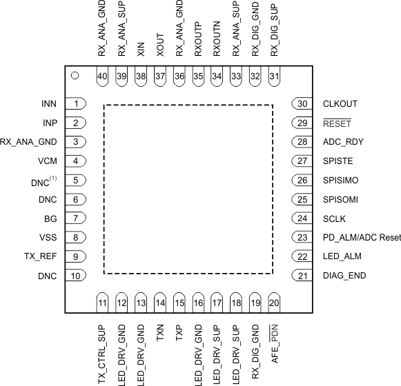
Pin Functions
| PIN | FUNCTION | DESCRIPTION | |
|---|---|---|---|
| NAME | NO. | ||
| ADC_RDY | 28 | Digital | Output signal that indicates ADC conversion completion. Can be connected to the interrupt input pin of an external microcontroller. |
| AFE_PDN | 20 | Digital | AFE-only power-down input; active low. Can be connected to the port pin of an external microcontroller. |
| BG | 7 | Reference | Decoupling capacitor for internal band-gap voltage to ground (2.2-µF decoupling capacitor to ground, expected voltage = 1.0 V). |
| CLKOUT | 30 | Digital | Buffered 4-MHz output clock output. Can be connected to the clock input pin of an external microcontroller. |
| DIAG_END | 21 | Digital | Output signal that indicates completion of diagnostics. Can be connected to the port pin of an external microcontroller. |
| DNC(1) | 5, 6, 10 | — | Do not connect these pins. Leave as open-circuit. |
| INN | 1 | Analog | Receiver input pin. Connect to photodiode anode. |
| INP | 2 | Analog | Receiver input pin. Connect to photodiode cathode. |
| LED_DRV_GND | 12, 13, 16 | Supply | LED driver ground pin, H-bridge. Connect to common board ground. |
| LED_DRV_SUP | 17, 18 | Supply | LED driver supply pin, H-bridge. Connect to an external power supply capable of supplying the large LED current, which is drawn by this supply pin. |
| LED_ALM | 22 | Digital | Output signal that indicates an LED cable fault. Can be connected to the port pin of an external microcontroller. |
| PD_ALM/ADC Reset | 23 | Digital | Output signal that indicates a PD sensor or cable fault. Can be connected to the port pin of an external microcontroller. In ADC bypass mode, the PD_ALM pin can be used to bring out the ADC reset signal. |
| RESET | 29 | Digital | AFE-only reset input, active low. Can be connected to the port pin of an external microcontroller. |
| RX_ANA_GND | 3, 36, 40 | Supply | Rx analog ground pin. Connect to common board ground. |
| RX_ANA_SUP | 33, 39 | Supply | Rx analog supply pin; 0.1-µF decoupling capacitor to ground |
| RX_DIG_GND | 19, 32 | Supply | Rx digital ground pin. Connect to common board ground. |
| RX_DIG_SUP | 31 | Supply | Rx digital supply pin; 0.1-µF decoupling capacitor to ground |
| RXOUTN | 34 | Analog | External ADC negative input when in ADC bypass mode |
| RXOUTP | 35 | Analog | External ADC positive input when in ADC bypass mode |
| SCLK | 24 | SPI | SPI clock pin |
| SPISIMO | 26 | SPI | SPI serial in master out |
| SPISOMI | 25 | SPI | SPI serial out master in |
| SPISTE | 27 | SPI | SPI serial interface enable |
| TX_CTRL_SUP | 11 | Supply | Transmit control supply pin (0.1-µF decoupling capacitor to ground) |
| TX_REF | 9 | Reference | Transmitter reference voltage, 0.75 V default after reset. Connect a 2.2-μF decoupling capacitor to ground. |
| TXN | 14 | Analog | LED driver out B, H-bridge output. Connect to LED. |
| TXP | 15 | Analog | LED driver out B, H-bridge output. Connect to LED. |
| VCM | 4 | Reference | Input common-mode voltage output. Connect a series resistor (1 kΩ) and a decoupling capacitor (10 nF) to ground. The voltage across the capacitor can be used to shield (guard) the INP, INN traces. Expected voltage = 0.9 V. |
| VSS | 8 | Supply | Substrate ground. Connect to common board ground. |
| XOUT | 37 | Digital | Crystal oscillator pins. Connect an external 8-MHz crystal between these pins with the correct load capacitor (as specified by vendor) to ground. |
| XIN | 38 | Digital | Crystal oscillator pins. Connect an external 8-MHz crystal between these pins with the correct load capacitor (as specified by vendor) to ground. |
(1) Leave pins as open circuit. Do not connect.