ZHCSAT7H December 2012 – October 2014 AFE4490
PRODUCTION DATA.
- 1 特性
- 2 应用范围
- 3 说明
- 4 修订历史记录
- 5 Device Comparison Table
- 6 Pin Configuration and Functions
- 7 Specifications
- 8 Detailed Description
- 9 Applications and Implementation
- 10Power-Supply Recommendations
- 11Layout
- 12器件和文档支持
- 13机械封装和可订购信息
10 Power-Supply Recommendations
The AFE4490 has two sets of supplies: the receiver supplies (RX_ANA_SUP, RX_DIG_SUP) and the transmitter supplies (TX_CTRL_SUP, LED_DRV_SUP). The receiver supplies can be between 2.0 V to 3.6 V whereas the transmitter supplies can be between 3.0 V to 5.25 V. Another consideration that determines the minimum allowed value of the transmitter supplies is the forward voltage of the LEDs being driven. The current source and switches inside the AFE require voltage headroom that mandates the transmitter supply to be a few hundred millivolts higher than the LED forward voltage. TX_REF is the voltage that governs the generation of the LED current from the internal reference voltage. Choosing the lowest allowed TX_REF setting reduces the additional headroom required but results in higher transmitter noise. Other than for the highest end clinical SPO2 applications, this extra noise resulting from a lower TX_REF setting might be acceptable.
The LED_DRV_SUP and TX_CTRL_SUP are recommended to be tied together to the same supply (between
3.0 V and 5.25 V). The external supply (connected to the common anode of the two LEDs) must be high enough to account for the forward drop of the LEDs as well as the voltage headroom required by the current source and switches inside the AFE. In most cases, this voltage is expected to fall below 5.25 V; thus the external supply can be the same as the LED_DRV_SUP. However, there might be cases (for instance when two LEDs are connected in series) where the voltage required on the external supply is higher than 5.25 V. Such a case must be handled with care to ensure that the voltage on the TXP and TXN pins stays less than 5.25 V and also never exceeds the supply voltage of LED_DRV_SUP, TX_CTRL_SUP by more than 0.3 V.
Many scenarios of power management are possible.
Case 1: LED forward voltage is such that a voltage of 3.3 V (for example) is acceptable on LED_DRV_SUP. In that case, a single 3.3-V supply can be used to drive all four pins (RX_ANA_SUP, RX_DIG_SUP, TX_CTRL_SUP, LED_DRV_SUP). Care must be taken to provide some isolation between the transmit and receive supplies because the LED_DRV_SUP carries the high switching current from the LEDs.
Case 2: A low-voltage supply (2.2 V for instance) is available in the system. In this case, a boost converter can be used to derive the voltage for the LED_DRV_SUP, as shown in Figure 137.
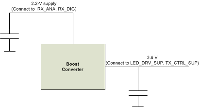 Figure 137. Boost Converter
The boost converter requires a clock (usually in the megahertz range) and there is usually a ripple at the boost converter output at this switching frequency. While this frequency is much higher than the signal frequency of interest (which is at maximum a few 10s of hertz around dc), a small fraction of this switching noise might possibly alias to the low-frequency band. Therefore, TI strongly recommends that the switching frequency of the boost converter be offset from every multiple of the PRF by at least 20 Hz, which can be ensured by choosing the appropriate PRF.
Case 3: In cases where a high voltage supply is available in the system, a buck converter or an LDO can be used to derive the voltage levels required to drive RX_ANA and RX_DIG. Such a scenario is shown in Figure 138.
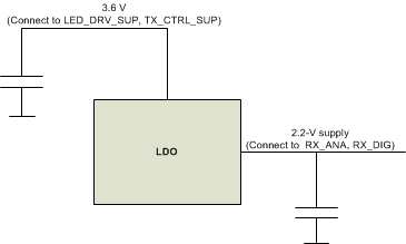 Figure 138. Buck Converter or an LDO
For more information on power-supply recommendations, see the AFE44x0SPO2EVM User's Guide (SLAU480).