ZHCSES1B March 2016 – October 2018 ADS1282-SP
PRODUCTION DATA.
- 1 特性
- 2 应用
- 3 说明
- 4 修订历史记录
- 5 (说明 (续))
- 6 Pin Configuration and Functions
-
7 Specifications
- 7.1 Absolute Maximum Ratings
- 7.2 ESD Ratings
- 7.3 Recommended Operating Conditions
- 7.4 Thermal Information
- 7.5 Electrical Characteristics
- 7.6 Timing Requirements
- 7.7 Pulse-Sync Timing Requirements
- 7.8 Reset Timing Requirements
- 7.9 Read Data Timing Requirements
- 7.10 Switching Characteristics
- 7.11 Typical Characteristics
-
8 Detailed Description
- 8.1 Overview
- 8.2 Functional Block Diagram
- 8.3
Feature Description
- 8.3.1 Noise Performance
- 8.3.2 Input-Referred Noise
- 8.3.3 Idle Tones
- 8.3.4 Operating Mode
- 8.3.5 Analog Inputs and Multiplexer
- 8.3.6 PGA (Programmable Gain Amplifier)
- 8.3.7 ADC
- 8.3.8 Modulator
- 8.3.9 Modulator Over-Range
- 8.3.10 Modulator Input Impedance
- 8.3.11 Modulator Over-Range Detection (MFLAG)
- 8.3.12 Voltage Reference Inputs (VREFP, VREFN)
- 8.3.13 Digital Filter
- 8.3.14 Master Clock Input (CLK)
- 8.3.15 Synchronization (SYNC Pin and Sync Command)
- 8.3.16 Pulse-Sync Mode
- 8.3.17 Continuous-Sync Mode
- 8.3.18 Reset (RESET Pin and Reset Command)
- 8.3.19 Power-Down (PWDN Pin and Standby Command)
- 8.3.20 Power-On Sequence
- 8.3.21 Serial Interface
- 8.3.22 Data Format
- 8.3.23 Reading Data
- 8.3.24 One-Shot Operation
- 8.4 Device Functional Modes
- 8.5
Programming
- 8.5.1
Commands
- 8.5.1.1 WAKEUP: Wake-Up from Standby Mode
- 8.5.1.2 STANDBY: Standby Mode
- 8.5.1.3 SYNC: Synchronize the A/D Conversion
- 8.5.1.4 RESET: Reset the Device
- 8.5.1.5 RDATAC: Read Data Continuous
- 8.5.1.6 SDATAC: Stop Read Data Continuous
- 8.5.1.7 RDATA: Read Data By Command
- 8.5.1.8 RREG: Read Register Data
- 8.5.1.9 WREG: Write to Register
- 8.5.1.10 OFSCAL: Offset Calibration
- 8.5.1.11 GANCAL: Gain Calibration
- 8.5.2 Calibration Commands
- 8.5.3 User Calibration
- 8.5.4 Configuration Guide
- 8.5.1
Commands
- 8.6 Register Maps
- 9 Application and Implementation
- 10Power Supply Recommendations
- 11Layout
- 12器件和文档支持
- 13机械、封装和可订购信息
8.3.17 Continuous-Sync Mode
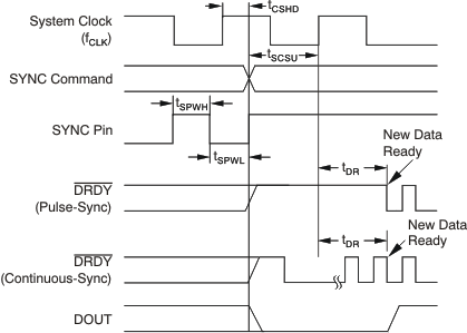
In Continuous-sync mode, either a single sync pulse or a continuous clock may be applied. When a single sync pulse is applied (rising edge), the device behaves similar to the Pulse-sync mode. However, in this mode, DRDY continues to toggle unaffected but the DOUT output is held low until data are ready, 63 DRDY periods later. When the conversion data are non-zero, new conversion data are ready (as shown in Figure 46).
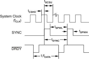
When a continuous clock is applied to the SYNC pin, the period must be an integral multiple of the output data rate or the device re-synchronizes. Synchronization results in the restarting of the digital filter and an interruption of 63 readings (refer to Pulse-Sync Timing Requirements).
When the sync input is first applied, the device re-synchronizes (under the condition tSYNC ≠ N / ƒDATA). DRDY continues to output but DOUT is held low until the new data are ready. Then, if SYNC is applied again and the period matches an integral multiple of the output data rate, the device freely runs without re-synchronization. The phase of the applied clock and output data rate (DRDY) are not matched because of the initial delay of DRDY after SYNC is first applied. Figure 47 shows the timing for Continuous-Sync mode.
A SYNC clock input should be applied after the Continuous-Sync mode is set. The first rising edge of SYNC then causes a synchronization.
 Figure 46. Pulse-Sync Timing, Continuous-Sync Timing With Single Sync
  Figure 47. Continuous-Sync Timing With Sync Clock