ZHCSCX0D January 2014 – October 2017 ADC12J1600 , ADC12J2700
PRODUCTION DATA.
- 1 特性
- 2 应用
- 3 说明
- 4 修订历史记录
- 5 Pin Configuration and Functions
- 6 Specifications
-
7 Detailed Description
- 7.1 Overview
- 7.2 Functional Block Diagram
- 7.3
Feature Description
- 7.3.1 Signal Acquisition
- 7.3.2 The Analog Inputs
- 7.3.3 Clocking
- 7.3.4 Over-Range Function
- 7.3.5 ADC Core Features
- 7.3.6
Digital Down Converter (DDC)
- 7.3.6.1 NCO/Mixer
- 7.3.6.2 NCO Settings
- 7.3.6.3 Decimation Filters
- 7.3.6.4 DDC Output Data
- 7.3.6.5 Decimation Settings
- 7.3.7
Data Outputs
- 7.3.7.1 The Digital Outputs
- 7.3.7.2
JESD204B Interface Features and Settings
- 7.3.7.2.1 Scrambler Enable
- 7.3.7.2.2 Frames Per Multi-Frame (K-1)
- 7.3.7.2.3 DDR
- 7.3.7.2.4 JESD Enable
- 7.3.7.2.5 JESD Test Modes
- 7.3.7.2.6 Configurable Pre-Emphasis
- 7.3.7.2.7 Serial Output-Data Formatting
- 7.3.7.2.8 JESD204B Synchronization Features
- 7.3.7.2.9 SYSREF
- 7.3.7.2.10 SYNC~
- 7.3.7.2.11 Time Stamp
- 7.3.7.2.12 Code-Group Synchronization
- 7.3.7.2.13 Multiple ADC Synchronization
- 7.4 Device Functional Modes
- 7.5 Programming
- 7.6
Register Map
- 7.6.1 Memory Map
- 7.6.2
Register Descriptions
- 7.6.2.1
Standard SPI-3.0 (0x000 to 0x00F)
- Table 40. Standard SPI-3.0 Registers
- 7.6.2.1.1 Configuration A Register (address = 0x000) [reset = 0x3C]
- 7.6.2.1.2 Configuration B Register (address = 0x001) [reset = 0x00]
- 7.6.2.1.3 Device Configuration Register (address = 0x002) [reset = 0x00]
- 7.6.2.1.4 Chip Type Register (address = 0x003) [reset = 0x03]
- 7.6.2.1.5 Chip Version Register (address = 0x006) [reset = 0x13]
- 7.6.2.1.6 Vendor Identification Register (address = 0x00C to 0x00D) [reset = 0x0451]
- 7.6.2.2 User SPI Configuration (0x010 to 0x01F)
- 7.6.2.3
General Analog, Bias, Band Gap, and Track and Hold (0x020 to 0x02F)
- 7.6.2.3.1 Power-On Reset Register (address = 0x021) [reset = 0x00]
- 7.6.2.3.2 I/O Gain 0 Register (address = 0x022) [reset = 0x40]
- 7.6.2.3.3 IO_GAIN_1 Register (address = 0x023) [reset = 0x00]
- 7.6.2.3.4 I/O Offset 0 Register (address = 0x025) [reset = 0x40]
- 7.6.2.3.5 I/O Offset 1 Register (address = 0x026) [reset = 0x00]
- 7.6.2.4
Clock (0x030 to 0x03F)
- 7.6.2.4.1 Clock Generator Control 0 Register (address = 0x030) [reset = 0xC0]
- 7.6.2.4.2 Clock Generator Status Register (address = 0x031) [reset = 0x07]
- 7.6.2.4.3 Clock Generator Control 2 Register (address = 0x032) [reset = 0x80]
- 7.6.2.4.4 Analog Miscellaneous Register (address = 0x033) [reset = 0xC3]
- 7.6.2.4.5 Input Clamp Enable Register (address = 0x034) [reset = 0x2F]
- 7.6.2.5 Serializer (0x040 to 0x04F)
- 7.6.2.6
ADC Calibration (0x050 to 0x1FF)
- 7.6.2.6.1 Calibration Configuration 0 Register (address = 0x050) [reset = 0x06]
- 7.6.2.6.2 Calibration Configuration 1 Register (address = 0x051) [reset = 0xF4]
- 7.6.2.6.3 Calibration Background Control Register (address = 0x057) [reset = 0x10]
- 7.6.2.6.4 ADC Pattern and Over-Range Enable Register (address = 0x058) [reset = 0x00]
- 7.6.2.6.5 Calibration Vectors Register (address = 0x05A) [reset = 0x00]
- 7.6.2.6.6 Calibration Status Register (address = 0x05B) [reset = undefined]
- 7.6.2.6.7 Timing Calibration Register (address = 0x066) [reset = 0x02]
- 7.6.2.7
Digital Down Converter and JESD204B (0x200-0x27F)
- 7.6.2.7.1 Digital Down-Converter (DDC) Control Register (address = 0x200) [reset = 0x10]
- 7.6.2.7.2 JESD204B Control 1 Register (address = 0x201) [reset = 0x0F]
- 7.6.2.7.3 JESD204B Control 2 Register (address = 0x202) [reset = 0x00]
- 7.6.2.7.4 JESD204B Device ID (DID) Register (address = 0x203) [reset = 0x00]
- 7.6.2.7.5 JESD204B Control 3 Register (address = 0x204) [reset = 0x00]
- 7.6.2.7.6 JESD204B and System Status Register (address = 0x205) [reset = Undefined]
- 7.6.2.7.7 Overrange Threshold 0 Register (address = 0x206) [reset = 0xF2]
- 7.6.2.7.8 Overrange Threshold 1 Register (address = 0x207) [reset = 0xAB]
- 7.6.2.7.9 Overrange Period Register (address = 0x208) [reset = 0x00]
- 7.6.2.7.10 DDC Configuration Preset Mode Register (address = 0x20C) [reset = 0x00]
- 7.6.2.7.11 DDC Configuration Preset Select Register (address = 0x20D) [reset = 0x00]
- 7.6.2.7.12 Rational NCO Reference Divisor Register (address = 0x20E to 0x20F) [reset = 0x0000]
- 7.6.2.7.13 NCO Frequency (Preset x) Register (address = see ) [reset = see ]
- 7.6.2.7.14 NCO Phase (Preset x) Register (address = see ) [reset = see ]
- 7.6.2.7.15 DDC Delay (Preset x) Register (address = see ) [reset = see ]
- 7.6.2.1
Standard SPI-3.0 (0x000 to 0x00F)
- 8 Application and Implementation
- 9 Power Supply Recommendations
- 10Layout
- 11器件和文档支持
- 12机械、封装和可订购信息
5 Pin Configuration and Functions
NKE Package
68-Pin VQFN With Thermal Pad
Top View
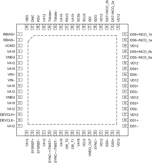
DNC = Make no external connection
Pin Functions
| PIN | EQUIVALENT CIRCUIT | TYPE | DESCRIPTION | |
|---|---|---|---|---|
| NAME | NO. | |||
| ANALOG | ||||
| RBIAS+ | 1 | 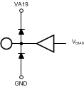 |
I/O | External Bias Resistor Connections External bias resistor terminals. A 3.3 kΩ (±0.1%) resistor should be connected between RBIAS+ and RBIAS–. The RBIAS resistor is used as a reference for internal circuits which affect the linearity of the converter. The value and precision of this resistor should not be compromised. These pins must be isolated from all other signals and grounds. |
| RBIAS– | 2 | |||
| TDIODE– | 63 |  |
Passive | Temperature Diode These pins are the positive (anode) and negative (cathode) diode connections for die temperature measurements. Leave these pins unconnected if they are not used. See the Built-In Temperature Monitor Diode section for more details. |
| TDIODE+ | 64 | |||
| VBG | 68 | 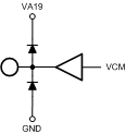 |
O | Bandgap Output Voltage This pin is capable of sourcing or sinking 100 μA and can drive a load up to 80 pF. Leave this pin unconnected if it is not used in the application. See the The Reference Voltage section for more details. |
| VCMO | 3 | O | Common Mode Voltage The voltage output at this pin must be the common-mode input voltage at the VIN+ and VIN– pins when DC coupling is used. This pin is capable of sourcing or sinking 100 μA and can drive a load up to 80 pF. Leave this pin unconnected if it is not used in the application. |
|
| VIN+ | 8 | 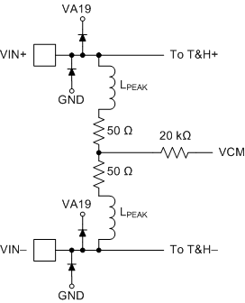 |
I | Signal Input The differential full-scale input range is determined by the full-scale voltage adjust register. An internal peaking inductor (LPEAK) of 5 nH is included for parasitic compensation. |
| VIN– | 9 | |||
| DATA | ||||
| DS0– | 32 | 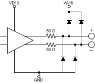 |
O | Data CML These pins are the high-speed serialized-data outputs with user-configurable pre-emphasis. These outputs must always be terminated with a 100-Ω differential resistor at the receiver. |
| DS0+ | 33 | |||
| DS1– | 35 | |||
| DS1+ | 36 | |||
| DS2– | 38 | |||
| DS2+ | 39 | |||
| DS3– | 41 | |||
| DS3+ | 42 | |||
| DS4– | 44 | |||
| DS4+ | 45 | |||
| DS5–/NCO_0 | 47 | 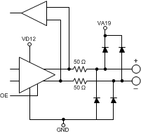 |
O/I | Data DS5–/NCO_0, DS5+/NCO_0, DS6–/NCO_1, DS6+/NCO_1, DS7–/NCO_2 and DS7+/NCO_2: When decimation is enabled, these pins become LVCMOS inputs and allow the host device to select the specific NCO frequency or phase accumulator that is active. In this mode the positive (+) and negative (–) pins should be connected together and both driven. An acceptable alternative is to let one of the pair float while the other pin is driven. Connect these inputs to GND if they are not used in the application. |
| DS5+/NCO_0 | 48 | |||
| DS6−/NCO_1 | 50 | |||
| DS6+/NCO_1 | 51 | |||
| DS7−/NCO_2 | 53 | |||
| DS7+/NCO_2 | 54 | |||
| GROUND, RESERVED, DNC | ||||
| DNC | 67 | — | Do Not Connect Do not connect DNC to any circuitry, power, or ground signals. |
|
| RSV | 66 |  |
— | Reserved Connect to Ground or Leave Unconnected: This reserved pin is a logic input for possible future device versions. It is recommended to connect this pin to ground. Floating this pin is also permissible. |
| RSV2 | 61 | — | Reserved Connect to Ground Connect this reserved input pin to ground for proper operation. |
|
| Thermal Pad | — | Ground (GND) The exposed pad on the bottom of the package is the ground return for all supplies. This pad must be connected with multiple vias to the printed circuit board (PCB) ground planes to ensure proper electrical and thermal performance. The exposed center pad on the bottom of the package must be thermally and electrically connected (soldered) to a ground plane to ensure rated performance. |
||
| LVCMOS | ||||
| OR_T0 | 25 |  |
O | Over-Range Over-range detection status for T0 and T1 thresholds. Leave these pins unconnected if they are not used in the application. |
| OR_T1 | 26 | |||
| SCLK | 58 |  |
I | Serial Interface Clock This pin functions as the serial-interface clock input which clocks the serial data in and out. The Using the Serial Interface section describes the serial interface in more detail. |
| SDI | 57 | I | Serial Data In This pin functions as the serial-interface data input. The Using the Serial Interface section describes the serial interface in more detail. |
|
| SYNC~ | 30 | I | SYNC~ This pin provides the JESD204B-required synchronizing request input. A logic-low applied to this input initiates a lane alignment sequence. The choice of LVCMOS or differential SYNC~ is selected through bit 6 of the configuration register 0x202h. Connect this input to GND or VA19 if differential SYNC~ input is used. |
|
| SCS | 59 | I | Serial Chip Select (active low) This pin functions as the serial-interface chip select. The Using the Serial Interface section describes the serial interface in more detail. |
|
| SDO | 56 |  |
O | Serial Data Out This pin functions as the serial-interface data output. The Using the Serial Interface section describes the serial interface in more detail. |
| DIFFERENTIAL INPUT | ||||
| DEVCLK+ | 15 | 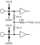 |
I | Device Clock Input The differential device clock signal must be AC coupled to these pins. The input signal is sampled on the rising edge of CLK. |
| DEVCLK– | 16 | |||
| SYSREF+ | 19 | I | SYSREF The differential periodic waveform on these pins synchronizes the device per JESD204B. If JESD204B subclass 1 synchronization is not required and these inputs are not utilized they may be left unconnected. In that case ensure SysRef_Rcvr_En=0 and SysRef_Pr_En=0. |
|
| SYSREF– | 20 | |||
| SYNC~+/TMST+ | 22 | I | SYNC~/TMST This differential input provides the JESD204B-required synchronizing request input. A differential logic-low applied to these inputs initiates a lane alignment sequence. For differential SYNC~ usage, ensure that SYNC_DIFF_PD = 0 and SYNC_DIFFSEL = 1. When the LVCMOS SYNC~ is selected these inputs can be used as the differential TIMESTAMP input. For TMST usage, ensure that SYNC_DIFF_PD = 0, SYNC_DIFFSEL = 0, and TIME_STAMP_EN = 1. For additional information see the Time Stamp section. These inputs may be left unconnected if they are not used for either the SYNC~ or TIMESTAMP functions. |
|
| SYNC~-/TMST– | 23 | |||
| POWER | ||||
| VA12 | 6 | — | Analog 1.2 V power supply pins Bypass these pins to ground using one 10-µF capacitor and two 1-µF capacitors for bulk decoupling plus one 0.1-µF capacitor per pin for individual decoupling. |
|
| 11 | ||||
| 14 | ||||
| 17 | ||||
| 18 | ||||
| 21 | ||||
| 65 | ||||
| VA19 | 4 | — | Analog 1.9 V power supply pins Bypass these pins to ground using one 10-µF capacitor and two 1-µF capacitors for bulk decoupling plus one 0.1-µF capacitor per pin for individual decoupling. |
|
| 7 | ||||
| 10 | ||||
| 13 | ||||
| 24 | ||||
| 27 | ||||
| 60 | ||||
| 62 | ||||
| VD12 | 28 | — | Digital 1.2 V power supply pins Bypass these pins to ground using one 10-µF capacitor and two 1-µF capacitors for bulk decoupling plus one 0.1-µF capacitor per pin for individual decoupling. |
|
| 31 | ||||
| 34 | ||||
| 37 | ||||
| 40 | ||||
| 43 | ||||
| 46 | ||||
| 49 | ||||
| 52 | ||||
| 55 | ||||
| VNEG | 5 | I | VNEG These pins must be decoupled to ground with a 0.1-µF ceramic capacitor near each pin. These power input pins must be connected to the VNEG_OUT pin with a low resistance path. The connections must be isolated from any noisy digital signals and must also be isolated from the analog input and clock input pins. |
|
| 12 | ||||
| VNEG_OUT | 29 | O | VNEG_OUT The voltage on this output can range from –1V to +1V. This pin must be decoupled to ground with a 4.7-µF, low ESL, low ESR multi-layer ceramic chip capacitor and connected to the VNEG input pins. This voltage must be isolated from any noisy digital signals, clocks, and the analog input. |
|