SNAS747 June 2017 ADC081S101-MIL
PRODUCTION DATA.
- 1 Features
- 2 Applications
- 3 Description
- 4 Revision History
- 5 Pin Configuration and Functions
- 6 Specifications
- 7 Typical Characteristics
- 8 Detailed Description
- 9 Applications Information
- 10Power Supply Recommendations
- 11Device and Documentation Support
- 12Mechanical, Packaging, and Orderable Information
9 Applications Information
NOTE
Information in the following applications sections is not part of the TI component specification, and TI does not warrant its accuracy or completeness. TI’s customers are responsible for determining suitability of components for their purposes. Customers should validate and test their design implementation to confirm system functionality.
9.1 Analog Input
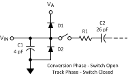
An equivalent circuit for the ADC's input channel is shown in Figure 22. Diodes D1 and D2 provide ESD protection for the analog inputs. At no time should any input go beyond (VA + 300 mV) or (GND − 300 mV), as these ESD diodes will begin conducting, which could result in erratic operation. For this reason, the ESD diodes should not be used to clamp the input signal.
The capacitor C1 in Figure 22 has a typical value of 4 pF, and is mainly the package pin capacitance. Resistor R1 is the on resistance of the multiplexer and track / hold switch, and is typically 500Ω. Capacitor C2 is the ADC sampling capacitor and is typically 26 pF. The ADC will deliver best performance when driven by a low-impedance source to eliminate distortion caused by the charging of the sampling capacitance. This is especially important when using the ADC to sample AC signals. Also important when sampling dynamic signals is an anti-aliasing filter.
 Figure 22. Equivalent Input Circuit
9.1.1 Digital Inputs And Outputs
The ADC digital inputs (SCLK and CS) are not limited by the same absolute maximum ratings as the analog inputs. The digital input pins are instead limited to +5.25V with respect to GND, regardless of VA, the supply voltage. This allows the ADC to be interfaced with a wide range of logic levels, independent of the supply voltage.
9.2 Typical Application Circuit
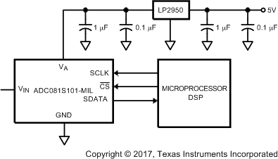
A typical application of the ADC is shown in Figure 23. Power is provided in this example by the TI LP2950 low-dropout voltage regulator, available in a variety of fixed and adjustable output voltages. The power supply pin is bypassed with a capacitor network located close to the ADC. Because the reference for the ADC is the supply voltage, any noise on the supply will degrade device noise performance. To keep noise off the supply, use a dedicated linear regulator for this device, or provide sufficient decoupling from other circuitry to keep noise off the ADC supply pin. Because of the ADC's low power requirements, it is also possible to use a precision reference as a power supply to maximize performance. The four-wire interface is also shown connected to a microprocessor or DSP.
 Figure 23. Typical Application Circuit