SNAS747 June 2017 ADC081S101-MIL
PRODUCTION DATA.
- 1 Features
- 2 Applications
- 3 Description
- 4 Revision History
- 5 Pin Configuration and Functions
- 6 Specifications
- 7 Typical Characteristics
- 8 Detailed Description
- 9 Applications Information
- 10Power Supply Recommendations
- 11Device and Documentation Support
- 12Mechanical, Packaging, and Orderable Information
1 Features
- Specified Over a Range of Sample Rates
- 6-Lead WSON and SOT-23 Packages
- Variable Power Management
- Single Power Supply with 2.7-V - 5.25-V Range
- SPI™/QSPI™/MICROWIRE/DSP Compatible
- DNL ± 0.07 LSB (typ)
- INL ± 0.05 LSB (typ)
- SNR 49.7 dB (typ)
- Power Consumption
- 3-V Supply 2.0 mW (typ)
- 5-V Supply 10.0 mW (typ)
2 Applications
- Portable Systems
- Remote Data Acquisitions
- Instrumentation and Control Systems
3 Description
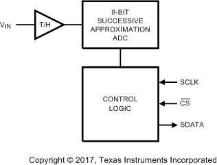
The ADC081S101-MIL is a low-power, single channel CMOS 8-bit analog-to-digital converter with a high-speed serial interface. Unlike the conventional practice of specifying performance at a single sample rate only, the ADC081S101-MIL is fully specified over a sample rate range of 500 ksps to 1 Msps. The converter is based upon a successive-approximation register architecture with an internal track-and-hold circuit.
The output serial data is straight binary, and is compatible with several standards, such as SPI™, QSPI™, MICROWIRE, and many common DSP serial interfaces.
The ADC081S101-MIL operates with a single supply that can range from 2.7 V to 5.25 V. Normal power consumption using a +3 V or +5 V supply is 2.0 mW and 10.0 mW, respectively. The power-down feature reduces the power consumption to just 2.5 µW using a +5 V supply.
The ADC081S101-MIL is packaged in an 6-lead WSON and SOT-23 packages. Operation over the industrial temperature range of −40°C to +85°C is ensured.
Device Information(1)
| PART NUMBER | PACKAGE | BODY SIZE (NOM) |
|---|---|---|
| ADC081S101-MIL | SOT-23 (6 DBV) | 2.90 x 1.60 mm |
| WSON (6 NGF) | 2.50 x 2.20 mm |
- For all available packages, see the orderable addendum at the end of the data sheet.
Block Diagram
