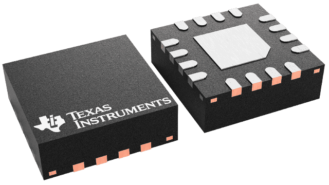
封装信息
| 封装 | 引脚 VQFN (RGT) | 16 |
| 工作温度范围 (°C) -40 to 85 |
| 包装数量 | 包装 3,000 | LARGE T&R |
PCA9554A 的特性
- I2C 至并行端口扩展器
- 开漏电路低电平有效中断输出
- 2.3 V 至 5.5V 的工作电源电压范围
- 耐受 5V 电压的 I/O
- 400kHz 快速 I2C 总线
- 3 个硬件地址引脚可在 I2C/SMBus 上支持最多 8 个器件
- 输入/输出配置寄存器
- 极性反转寄存器
- 内部加电复位
- 所用通道在加电时被配置为输入
- 加电时无毛刺脉冲
- 针对直接驱动 LED 的具有高电流驱动最大能力的锁存输出
- 锁断性能超过 100mA,符合 JESD 78 II 类规范的要求)
- ESD 保护性能超过 JESD 22 规范要求
- 2000V 人体放电模型 (A114-A)
- 200V 机器放电模型 (A115-A)
- 1000V 带电器件模型 (C101)
PCA9554A 的说明
The PCA9554A open-drain interrupt ( INT) output is activated when any input state differs from its corresponding Input Port register state and is used to indicate to the system master that an input state has changed.
INT can be connected to the interrupt input of a microcontroller. By sending an interrupt signal on this line, the remote I/O can inform the microcontroller if there is incoming data on its ports without having to communicate via the I2C bus. Thus, the PCA9554A can remain a simple slave device.
The device’s outputs (latched) have high-current drive capability for directly driving LEDs and low current consumption.
Three hardware pins (A0, A1, and A2) are used to program and vary the fixed I2C address and allow up to eight devices to share the same I2C bus or SMBus.
The PCA9554A is pin-to-pin and I2C address compatible with the PCF8574A. However, software changes are required, due to the enhancements in the PCA9554A over the PCF8574A.
The PCA9554A and PCA9554 are identical except for their fixed I2C address. This allows for up to 16 of these devices (8 of each) on the same I2C/SMBus.