SLVSA08A February 2010 – September 2015 TPS657052
PRODUCTION DATA.
- 1 Features
- 2 Applications
- 3 Description
- 4 Revision History
- 5 Device Options
- 6 Pin Configuration and Functions
- 7 Specifications
- 8 Detailed Description
- 9 Application and Implementation
- 10Power Supply Recommendations
- 11Layout
- 12Device and Documentation Support
- 13Mechanical, Packaging, and Orderable Information
1 Features
- Two 400-mA Step-Down Converters
- Up to 92% Efficiency
- VIN Range for DC-DC Converter
From 3.3 V to 6 V - 2.25-MHz Fixed-Frequency Operation
- Power Save Mode at Light Load Current
- Output Voltage Accuracy in PWM Mode ±1.5%
- 100% Duty Cycle for Lowest Dropout
- 180° Out-of-Phase Operation
- 1 General Purpose 200-mA LDO
- VIN Range for LDO From 1.7 V to 6.0 V
- Available in a 16-Ball DSBGA (WCSP) With 0.5-mm Pitch
2 Applications
- Digital Cameras
- Portable Media Players
- Handheld Equipment
3 Description
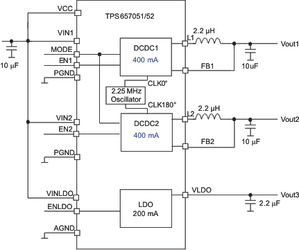
The TPS65705x devices are small power management units targeted for embedded camera module or other portable low-power consumer-end equipments. The device contains two highly efficient step-down converters, a low dropout linear regulator, and additional supporting functions. The 2.25-MHz step-down converter enters a low-power mode at light load for maximum efficiency across the widest possible range of load currents. For low-noise applications, the device can be forced into fixed-frequency PWM mode using the MODE pin. The device allows the use of small inductors and capacitors to achieve a small sized solution. The TPS65705x provides an output current of up to
400 mA on both DC-DC converters and integrates one 200-mA LDO with different output settings. The LDO operates with an input voltage range from 1.7 V to 6 V, thus allowing it to be supplied from the output of the step-down converter or directly from the system voltage.
The TPS65705x comes in a small 16-pin wafer chip scale package (WCSP) with 0.5-mm ball pitch.
Device Information(1)
| PART NUMBER | PACKAGE | BODY SIZE (NOM) |
|---|---|---|
| TPS657051 | DSBGA (16) | 2.08 mm × 2.08 mm |
| TPS657052 |
- For all available packages, see the orderable addendum at the end of the data sheet.
Application Circuit
