SLVSA08A February 2010 – September 2015 TPS657052
PRODUCTION DATA.
- 1 Features
- 2 Applications
- 3 Description
- 4 Revision History
- 5 Device Options
- 6 Pin Configuration and Functions
- 7 Specifications
- 8 Detailed Description
- 9 Application and Implementation
- 10Power Supply Recommendations
- 11Layout
- 12Device and Documentation Support
- 13Mechanical, Packaging, and Orderable Information
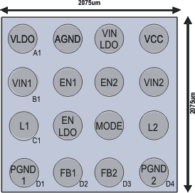
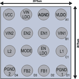
6 Pin Configuration and Functions
TPS657051 YZH Package
16-Pin DSBGA
Top View

TPS657052 YZH Package
16-Pin DSBGA
Top View

Pin Functions
| PIN | I/O | DESCRIPTION | |
|---|---|---|---|
| NO. | NAME | ||
| A1 | VLDO | O | Output voltage from LDO |
| A2 | AGND | — | Analog ground |
| A3 | VINLDO | I | Input voltage pin for LDO |
| A4(1) | VCC | I | Supply Input for internal reference, has to be connected to VIN1/ VIN2 |
| B1(2) | VIN1 | I | Input voltage pin for buck converter 1 |
| B2 | EN1 | I | Actively high enable input voltage for buck converter 1 |
| B3 | EN2 | I | Actively high enable input voltage for buck converter 2 |
| B4(2) | VIN2 | I | Input voltage pin for buck converter 2 |
| C1 | L1 | O | Switch output from buck converter 1 |
| C2 | ENLDO | I | Actively high enable input voltage for LDO |
| C3 | MODE | I | Set low to enable Power Save Mode. Pulling this PIN to high forces the device to operate in PWM mode over the whole load range. |
| C4 | L2 | O | Switch output from buck converter 2 |
| D1 | PGND1 | — | Power ground |
| D2 | FB1 | I | Feedback input from buck converter 1 |
| D3 | FB2 | I | Feedback input from buck converter 2 |
| D4 | PGND2 | — | Power ground |
(1) VCC must be the highest input for the device to function correctly.
(2) VIN1/VIN2 must be connected to VCC.