SLVSA08A February 2010 – September 2015 TPS657052
PRODUCTION DATA.
- 1 Features
- 2 Applications
- 3 Description
- 4 Revision History
- 5 Device Options
- 6 Pin Configuration and Functions
- 7 Specifications
- 8 Detailed Description
- 9 Application and Implementation
- 10Power Supply Recommendations
- 11Layout
- 12Device and Documentation Support
- 13Mechanical, Packaging, and Orderable Information
8 Detailed Description
8.1 Overview
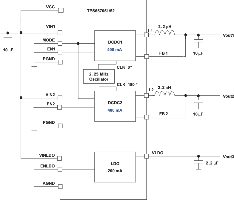
The TPS65705x integrates fixed-output voltage, two highly efficient step-down converters, along with an LDO. Each regulator has dedicated input pins for easy control.
8.2 Functional Block Diagram

8.3 Feature Description
8.3.1 DC-DC Converter
The TPS65705x step-down converter operates with typically 2.25-MHz fixed-frequency pulse width modulation (PWM) at moderate to heavy load currents. With MODE pin set to low, at light load currents the converter can automatically enter Power Save Mode and operates then in PFM mode.
During PWM operation the converter use a unique fast response voltage mode control scheme with input voltage feed-forward to achieve good line and load regulation allowing the use of small ceramic input and output capacitors. At the beginning of each clock cycle initiated by the clock signal, the high-side MOSFET switch is turned on. The current flows now from the input capacitor through the high-side MOSFET switch through the inductor to the output capacitor and load. During this phase, the current ramps up until the PWM comparator trips and the control logic will turn off the switch. The current limit comparator will also turn off the switch in case the current limit of the high-side MOSFET switch is exceeded. After an off time preventing shoot through current, the low-side MOSFET rectifier is turned on and the inductor current will ramp down. The current flows now from the inductor to the output capacitor and to the load. It returns back to the inductor through the low-side MOSFET rectifier.
The next cycle will be initiated by the clock signal again turning off the low-side MOSFET rectifier and turning on the on the high-side MOSFET switch. The DCDC1 converter output voltage is set to 3.3 V and the DCDC2 converter output voltage is set to 1.8 V per default. A 180° phase shift between DCDC1 and DCDC2 decreases the input RMS current and synchronizes the operation of the two DC-DC converts. The FB pin must be directly connected to the output voltage of DC-DC and no external resistor network must be connected.
8.3.2 Power Save Mode
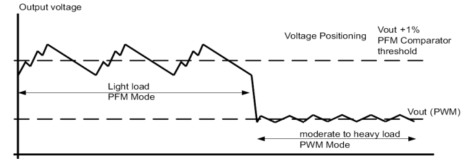
The Power Save Mode is enabled with Mode Pin set to low. If the load current decreases, the converter will enter Power Save Mode operation automatically. During Power Save Mode the converter skips switching and operates with reduced frequency in PFM mode with a minimum quiescent current to maintain high efficiency. The converter will position the output voltage typically +1% above the nominal output voltage. This voltage positioning feature minimizes voltage drops caused by a sudden load step. The transition from PWM mode to PFM mode occurs once the inductor current in the low-side MOSFET switch becomes zero, which indicates discontinuous conduction mode. During the Power Save Mode the output voltage is monitored with a PFM comparator. As the output voltage falls below the PFM comparator threshold of VOUT nominal +1%, the device starts a PFM current pulse. The high-side MOSFET switch will turn on, and the inductor current ramps up. After the ON-time expires, the switch is turned off and the low-side MOSFET switch is turned on until the inductor current becomes zero. The converter effectively delivers a current to the output capacitor and the load. If the load is below the delivered current, the output voltage will rise. If the output voltage is equal or higher than the PFM comparator threshold, the device stops switching and enters a sleep mode with typical 25-µA current consumption.
If the output voltage is still below the PFM comparator threshold, a sequence of further PFM current pulses are generated until the PFM comparator threshold is reached. The converter starts switching again once the output voltage drops below the PFM comparator threshold. With a fast single threshold comparator, the output voltage ripple during PFM mode operation can be kept small. The PFM Pulse is time controlled, which allows to modify the charge transferred to the output capacitor by the value of the inductor. The resulting PFM output voltage ripple and PFM frequency depend in first order on the size of the output capacitor and the inductor value. Increasing output capacitor values and inductor values will minimize the output ripple. The PFM frequency decreases with smaller inductor values and increases with larger values. The PFM mode is left and PWM mode is entered in case the output current can not longer be supported in PFM mode. The Power Save Mode can be disabled by setting Mode pin to high. The converter will then operate in fixed-frequency PWM mode.
8.3.2.1 Dynamic Voltage Positioning
This feature reduces the voltage under/overshoots at load steps from light to heavy load and vice versa. It is active in Power Save Mode and regulates the output voltage 1% higher than the nominal value. This provides more headroom for both the voltage drop at a load step, and the voltage increase at a load throw-off.

8.3.2.2 Soft Start
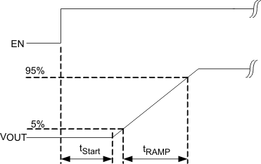
The step-down converter in TPS657051/52 has an internal soft start circuit that controls the ramp up of the output voltage. The output voltage ramps up from 5% to 95% of its nominal value within typical 250s. This limits the inrush current in the converter during ramp up and prevents possible input voltage drops when a battery or high impedance power source is used.
 Figure 21. Soft Start
8.3.2.3 100% Duty Cycle Low Dropout Operation
The device starts to enter 100% duty cycle mode once the input voltage comes close to the nominal output voltage. In order to maintain the output voltage, the high-side MOSFET switch is turned on 100% for one or more cycles. With further decreasing VIN the high-side MOSFET switch is turned on completely. In this case the converter offers a low input-to-output voltage difference. This is particularly useful in battery-powered applications to achieve longest operation time by taking full advantage of the whole battery voltage range. The minimum input voltage to maintain regulation depends on the load current and output voltage, and can be calculated as:
where
- IOmax = maximum output current plus inductor ripple current
- RDS(on)max = maximum high-side switch RDSon
- RL = DC resistance of the inductor
- VOmax = nominal output voltage plus maximum output voltage tolerance
8.3.3 180° Out-of-Phase Operation
In PWM Mode the converters operate with a 180° turn-on phase shift of the PMOS (high-side) transistors. This prevents the high-side switches of both converters from being turned on simultaneously, and therefore smooths the input current. This feature reduces the surge current drawn from the supply.
8.3.3.1 Under-Voltage Lockout
The under voltage lockout circuit prevents the device from malfunctioning at low input voltages and from excessive discharge of the battery and disables the converters and LDOs. The under-voltage lockout threshold is typically 2.2 V.
8.3.4 Short-Circuit Protection
All outputs are short-circuit protected with a maximum output current as defined in the electrical specifications.
8.3.5 Thermal Shutdown
As soon as the junction temperature, TJ, exceeds typically 150°C for the DC-DC converter or LDO, the device goes into thermal shutdown. In this mode, the low-side and high-side MOSFETs are turned-off. The device continues its operation when the junction temperature falls below the thermal shutdown hysteresis again. A thermal shutdown for the LDO or the DC-DC converter will disable both power supplies simultaneously.
8.3.6 LDO
The low dropout voltage regulator is designed to operate well with low value ceramic input and output capacitors. It operates with input voltages down to 1.7 V. The LDO offers a maximum dropout voltage of 200 mV at rated output current. The LDO supports a current limit feature.
8.3.7 Enable for DCDC1, DCDC2 and LDO
Disabling the DC-DC converter or LDO, forces the device into shutdown, with a shutdown quiescent current as defined in Electrical Characteristics. In this mode, the power FETs are turned-off and the entire internal control circuitry is switched-off.
8.4 Device Functional Modes
DCDC1, DCDC2, and LDO have dedicated enable pins. If all enable pins are pulled low the device will remain shutdown. If any of enable pins are pulled high corresponding regulators are enabled.