SLOS670B November 2010 – December 2016 TAS5727
PRODUCTION DATA.
- 1 Features
- 2 Applications
- 3 Description
- 4 Revision History
- 5 Description (continued)
- 6 Device Comparison Table
- 7 Pin Configuration and Functions
-
8 Specifications
- 8.1 Absolute Maximum Ratings
- 8.2 ESD Ratings
- 8.3 Recommended Operating Conditions
- 8.4 Thermal Information
- 8.5 DC Electrical Characteristics
- 8.6 AC Electrical Characteristics (BTL, PBTL)
- 8.7 PLL Input Parameters and External Filter Components
- 8.8 Serial Audio Ports Slave Mode
- 8.9 I2C Serial Control Port Operation
- 8.10 Reset Timing (RESET)
- 8.11 Typical Characteristics
- 9 Parameter Measurement Information
-
10Detailed Description
- 10.1 Overview
- 10.2 Functional Block Diagrams
- 10.3
Feature Description
- 10.3.1 Power Supply
- 10.3.2 I2C Address Selection and Fault Output
- 10.3.3 Device Protection Systems
- 10.3.4 Clock, Auto Detection, and PLL
- 10.3.5 PWM Section
- 10.3.6 SSTIMER Functionality
- 10.3.7 Single-Filter PBTL Mode
- 10.3.8 I2C Serial Control Interface
- 10.3.9 Audio Serial Interface
- 10.3.10 Serial Interface Control and Timing
- 10.3.11 Dynamic Range Control (DRC)
- 10.3.12 PWM Level Meter
- 10.4 Device Functional Modes
- 10.5 Programming
- 10.6
Register Maps
- 10.6.1 Clock Control Register (0x00)
- 10.6.2 Device Id Register (0x01)
- 10.6.3 Error Status Register (0x02)
- 10.6.4 System Control Register 1 (0x03)
- 10.6.5 Serial Data Interface Register (0x04)
- 10.6.6 System Control Register 2 (0x05)
- 10.6.7 Soft Mute Register (0x06)
- 10.6.8 Volume Registers (0x07, 0x08, 0x09)
- 10.6.9 Volume Configuration Register (0x0E)
- 10.6.10 Modulation Limit Register (0x10)
- 10.6.11 Interchannel Delay Registers (0x11, 0x12, 0x13, and 0x14)
- 10.6.12 PWM Shutdown Group Register (0x19)
- 10.6.13 Start/Stop Period Register (0x1A)
- 10.6.14 Oscillator Trim Register (0x1B)
- 10.6.15 BKND_ERR Register (0x1C)
- 10.6.16 Input Multiplexer Register (0x20)
- 10.6.17 Channel 4 Source Select Register (0x21)
- 10.6.18 PWM Output MUX Register (0x25)
- 10.6.19 DRC Control Register (0x46)
- 10.6.20 PWM Switching Rate Control Register (0x4F)
- 10.6.21 Bank Switch and EQ Control (0x50)
-
11Application and Implementation
- 11.1 Application Information
- 11.2
Typical Applications
- 11.2.1 Stereo Stereo Bridge Tied Load Application
- 11.2.2 Mono Parallel Bridge Tied Load Application
- 12Power Supply Recommendations
- 13Layout
- 14Device and Documentation Support
- 15Mechanical, Packaging, and Orderable Information
1 Features
-
Audio Input and Output
- 25 W Into an 8-Ω Load From a 20-V Supply
- Wide PVDD Range, From 8 V to 26 V
- Supports BTL Configuration With 4-Ω Load
- Efficient Class-D Operation Eliminates Need for Heatsinks
- One Serial Audio Input (Two Audio Channels)
- I2C Address Selection Pin (Chip Select)
- Single Output Filter PBTL Support
- Supports 44.1-kHz to 48-kHz Sample Rate (LJ/RJ/I2S)
- Audio and PWM Processing
- Independent Channel Volume Controls With Gain of 24 dB to Mute With 0.125-dB Resolution Steps
- Programmable Two-Band Dynamic-Range Control
- 18 Programmable Biquads for Speaker EQ and Other Audio-Processing Features
- Programmable Coefficients for DRC Filters
- DC Blocking Filters
- General Features
- I2C Serial Control Interface Operational Without MCLK
- Requires Only 3.3 V and PVDD
- No External Oscillator: Internal Oscillator for Automatic Rate Detection
- Surface-Mount, 48-Pin HTQFP Package
- Thermal and Short-Circuit Protection
- 106-dB SNR, A-Weighted
- AD, BD, and Ternary Modulation
- Up to 90% Efficient
- PWM Level Meter to Measure the Digital Power Profile
- Benefits
- EQ: Speaker Equalization Improves Audio Performance
- Two-Band DRC: Dynamic Range Compression. Can Be Used As Power Limiter. Enables Speaker Protection, Easy Listening, Night-Mode Listening
- Autodetect: Automatically Detects Sample-Rate Changes. No Need for External Microprocessor Intervention
2 Applications
- LCD TV, LED TV, Soundbar
3 Description
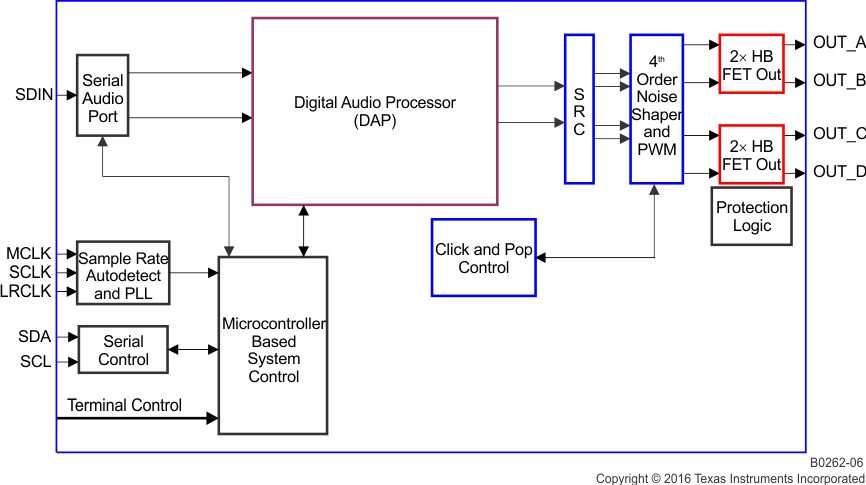
The TAS5727 is a 25-W, efficient, digital-audio power amplifier for driving stereo bridge-tied speakers. One serial data input allows processing of up to two discrete audio channels and seamless integration to most digital audio processors and MPEG decoders. The device accepts a wide range of input data and data rates. A fully programmable data path routes these channels to the internal speaker drivers.
Device Information(1)
| PART NUMBER | PACKAGE | BODY SIZE (NOM) |
|---|---|---|
| TAS5727 | HTQFP (48) | 7.00 mm × 7.00 mm |
- For all available packages, see the orderable addendum at the end of the data sheet.
Functional View
