SLUAAM3 August 2022 LM5113-Q1 , LMG1020 , LMG1025-Q1 , LMG1205 , LMG1210 , UCC27611
Gate drivers incorporate short propagation delays and powerful output stages capable of delivering large current peaks with quick rise and fall times at the gate of the FET for quick voltage changes. Having a proper schematic and layout is very important in a high current, fast switching circuit to attain the appropriate device operation. A good schematic and layout will help reduce any parasitics that might be present in the circuit. The recommendations that are provided can help improve the performance of the circuit and device. Typical values all subsequent components can be found on any of the corresponding devices data sheet.
Half-Bridge Driver Schematic Tips
A typical half bridge schematic is shown in Figure 1-1. The figure shows a summary of the components that are recommended for a half bridge driver. The colors are organized to represent the power supply, input, bootstrap circuit, and output recommendations.
The red section in Figure 1-1 shows the recommendations for the power supply. For a typical half-bridge driver, it is important to have two bypass capacitors at VDD. TI recommends having one larger capacitor to reduce the VDD drop at turn on and to charge the bootstrap capacitor. A second smaller capacitor is also recommended to reduce any noise that may be present at the VDD pin.
The inputs of the driver are shown in the yellow section of Figure 1-1. The general recommendation is to avoid any input filtering at the input stage. Input filtering would slow down the signal too much which is not ideal for high speed applications. In applications where speed is not a huge factor, adding an input filter can help clean up the input signal.
Next are the considerations for the bootstrap circuit which corresponds to the green section in Figure 1-1. This circuit serves as a high-side bias to drive the high side FET. The bootstrap capacitor will drive the high side gate which charges when the low side gate is on. When the low side FET is off, the bootstrap capacitor will be used to drive the high side FET. When building the bootstrap circuit, a good rule to follow is to use a bootstrap capacitor with a value that is equal to or greater than 10x the FET’s gate capacitance. The VDD bypass capacitor should also be equal to or greater than 10x the bootstrap capacitor. Equally important is the bootstrap diode, which helps reduce the risk of current being supplied back to the driver supply from the bootstrap capacitor. The bootstrap diode should be a fast reverse recovery or Schottky diode rated higher than the max bootstrap voltage. When using an external bootstrap diode, the use of a bootstrap resistor can help reduce the current flowing through the diode. Keep in mind that some devices tend to have internal bootstrap components, so it is important to check the device specifications before designing the bootstrap circuit.
At the output stage of a half-bridge driver there will generally be two FETs: one on the high side and one on the low side, as shown in the blue section of Figure 1-1. The low side output drives the ground referenced FET whose gate voltage will be equal to VDD. The high side output is a floating driver with HS as a reference. The gate voltage for this FET will be equal to VDD minus the boot diodes forward voltage drop with respect to HS. The resistors at the outputs are there to control the switch on and switch off speeds as well as to help limit noise and ringing in the gate drive path.
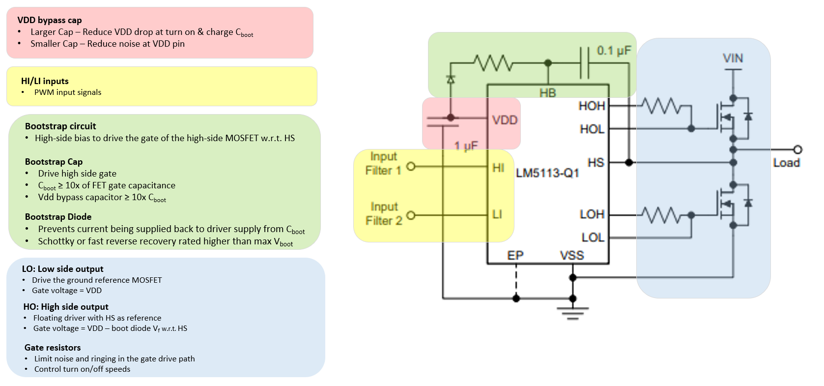 Figure 1-1 Summary of Half-Bridge
Components
Figure 1-1 Summary of Half-Bridge
ComponentsLow Side Driver Tips
A typical low side driver schematic is shown in Figure 1-2. It shows a summary of the components that are recommended for a low side driver. The colors are organized to represent the power supply, input, and output recommendations.
The red section in Figure 1-2 represents the power supply recommendations. TI recommends the use of two bypass capacitors, one with a larger capacitance value and a second one with a smaller capacitance value. The larger capacitor is needed to provide additional energy to minimize the voltage drop on VDD. The smaller value capacitors have a lower impedance at high frequencies and help reduce noise on the VDD pin.
Next is the input stage recommendations that are shown in the yellow section in Figure 1-2. Some low side drivers have the option of having two inputs. Typically, these two inputs are there to provide the option of using a non-inverting or inverting configuration which is shown by the IN+ and IN- pins in Figure 1-2. The input pins can also serve as an enable function. This can be done by connecting IN- to ground for a non-inverting input or connecting IN+ to VDD for an inverting input. It is also important to note that some devices have a safety feature that will not allow a floating input pin, so if this occurs the device will keep the output low until both pins are connected to something. Another thing to note is that for high speed applications, an input buffer can be used to generate 1ns pulses.
Lastly, the output stage is represented by the blue section in Figure 1-2. TI’s single channel GaN drivers provide a split-output configuration. Split output configuration allows for individual turn on and turn off time optimization of the FET. There are also gate resistors which help control turn on and turn off speeds while limiting the amount of noise and ringing in the gate drive path.
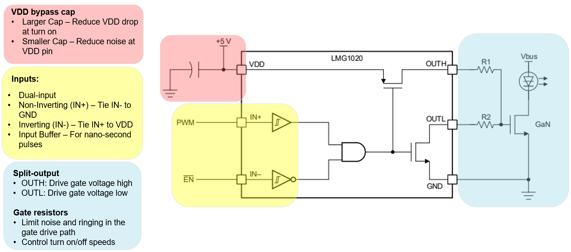 Figure 1-2 Summary of Low-Side
Components
Figure 1-2 Summary of Low-Side
ComponentsLayout Recommendations
A good layout helps reduce the amount of parasitic inductances or capacitances in the design. When designing with GaN drivers the board is required to have a minimum of four layers. A few general recommendations to consider are to parallel the source and return traces for flux cancellation, have separate signal and power traces, and to place the FETs close to the driver. These tips along with the rest that follow can help reduce number of parasitics that can be present in the design.
The recommendations that are shown for the layout are for a half bridge driver. The recommendations for half bridge drivers also apply to low side drivers. The first thing to consider is that the VDD bypass capacitor needs to be placed as close to the IC as possible. The smaller bypass capacitor needs to be the closest to the IC followed by the larger one. Figure 1-3 shows a good layout on the left vs. a bad layout on the right. The good layout has the bypass capacitor placed close to the IC whereas the bad layout shows that the capacitor is quite far from the IC and can lead to performance issues.
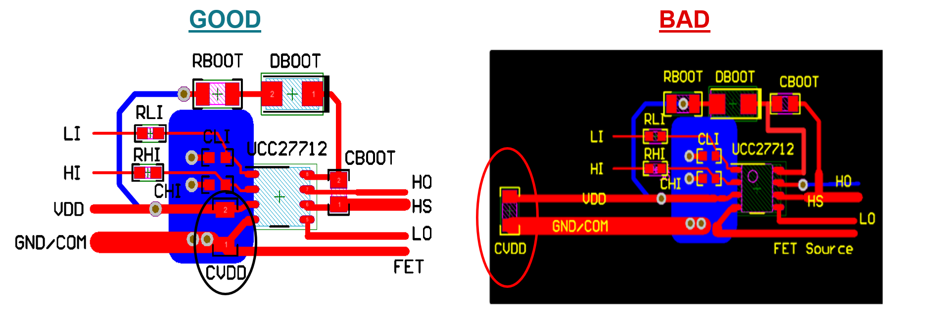 Figure 1-3 Comparison of Bypass Capacitor
Placements
Figure 1-3 Comparison of Bypass Capacitor
PlacementsThe use of short and wide traces in the bootstrap circuit path is preferred. The bootstrap circuit path is the path shown in Figure 1-4 and includes the bypass capacitor, the bootstrap resistor, the bootstrap diode, and the bootstrap capacitor. Using short and wide traces helps minimize parasitic inductances on the VDD trace. Additionally, placing the bootstrap capacitor as close as possible to the HB and HS pins helps to improve performance.
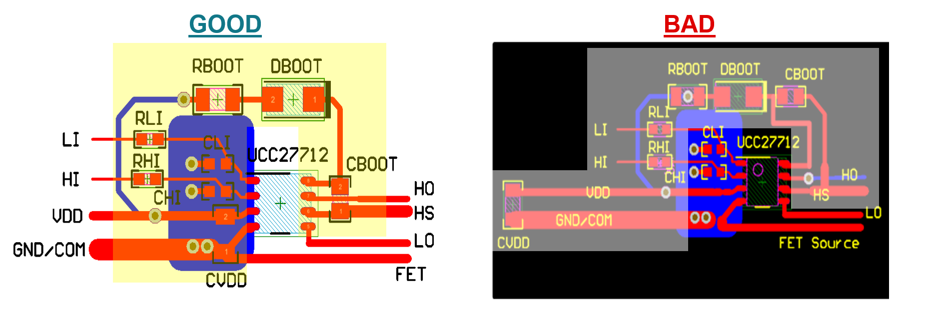 Figure 1-4 Bootstrap Circuit Path
When placing components at the inputs LI and HI, place them as close to the gate driver IC as possible while also keeping the placement and traces symmetrical, as shown in Figure 1-4.
At the output stage, minimizing the high current gate drive loops will be beneficial. Since the outputs carry high current, it is important to minimize the output loop to avoid any parasitics. The loop is shown by the red circle on the left picture in Figure 1-5. The black line on the picture on the right in Figure 1-5 shows another view of the gate drive loop. Also important to note is that the driver output ground and power FET source need to be as short as possible. When designing a circuit following these recommendations can help improve the performance of the circuit which is why it is important to keep these considerations in mind.
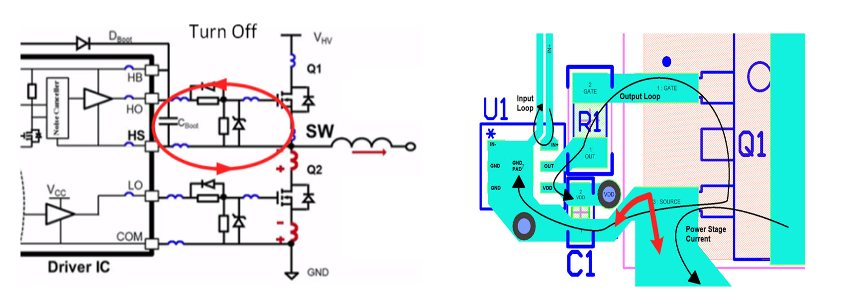 Figure 1-5 Current Gate Drive
Loop