SLUAAM2 August 2022 LM5113-Q1 , LMG1020 , LMG1025-Q1 , LMG1205 , LMG1210 , UCC27611
Gate drivers are applicable in a wide variety of industry applications. The introduction of GaN has allowed many of these applications to experience improved performance by enabling designers to create more efficient and compact designs that can be driven at higher frequencies. This application brief provides some details of industry applications that have benefited from GaN and how they have improved.
LIDAR Application
Light detection and ranging (LIDAR) has many applications and can be used in automotive, robotics, drones, range finders, retinal imagers, surveying equipment, speed measurement devices, and much more.
LIDAR operates by using light in the form of a pulsed laser to detect objects and map their distances, which is why it is sometimes referred to as time of flight. There is a transmission system that sends out a short high-current light pulse. This pulse will bounce off of objects and eventually return to a receiver. The time between the signal leaving and returning can then be used to calculate the distance the pulse traveled. Transmitting signals faster will result in more accurate results since more data can be interpreted by the receiver. Gate drivers help send multiple pulses at very high speeds since they can operate at high frequencies.
 Figure 1-1 LIDAR Transmission and Receiver Functionality
Low side drivers tend to be common for LIDAR applications. Two recommended gate drivers for LIDAR are the LMG1020 and LMG1025-Q1 GaN gate drivers. These two gate drivers are ideal for GaN applications since they are capable of high frequency applications, ns pulse widths, and have a short propagation delay. They are able to drive a FET to produce a <1.5-ns laser optical pulse in excess of 100 W, making them great for LIDAR applications. Figure 1-2 shows a block diagram of a general LIDAR application from the TIDA-01573 reference design. Some of the key components include a pulse shortening buffer for to create ns pulse widths, the GaN gate driver, the GaN FET, and the laser diode. The driver will pulse the FET on and off so that the laser diode can send multiple pulses to map objects and their distances.
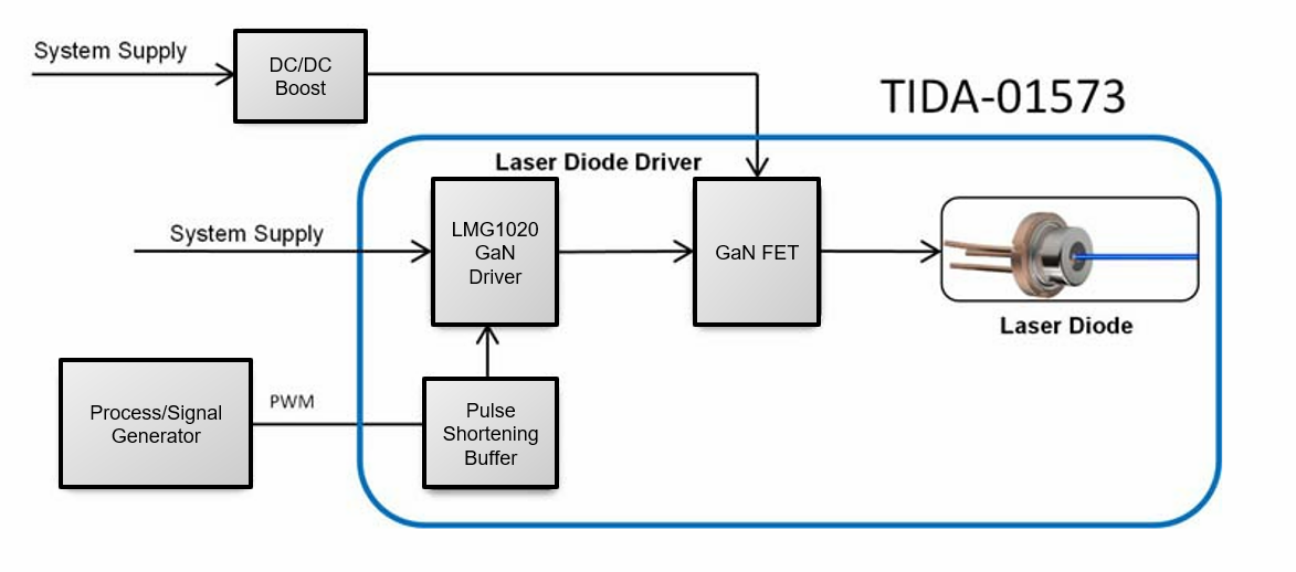 Figure 1-2 TIDA-01573 Reference Design Block Diagram
The schematic for TIDA-01573 reference design is shown in Figure 1-3. The LDO takes a VDD voltage input from 5.5 V – 15 V and provides a 5 V output, which is then used as a voltage supply to power up the driver. One key piece from this schematic is the addition of an input buffer which is needed to create ns pulse widths. The output of the driver is then connected to the gate of a GaN FET. Lastly, the load of the laser diode is represented by R5-R8.
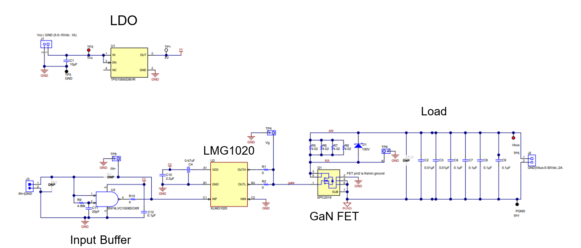 Figure 1-3 TIDA-01573 LIDAR Schematic
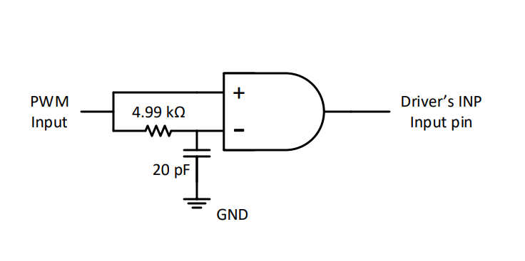 Figure 1-4 Input Buffer for Nano Second Pulses
Creation of Nanosecond Pulse Widths
This section explains how the input buffer from the schematic works. Figure 1-4 shows a close up view of the input buffer. In this case, the INM pin of the driver in Figure 1-3 is tied to ground to serve as an enable, therefore the output of the driver will be high whenever the INP signal goes high. This method requires an RC filter and an AND gate. The PWM signal is connected directly to AND+. Then there is a RC filter placed between the PWM signal and AND- which delays the signal that goes into the AND- pin. When the PWM input signal is high, the AND gate’s positive input will also be high, whereas the signal at the AND gate’s negative input will gradually increase as it will be affected by the RC filter connected between the PWM signal and the AND gate’s input.
A timing diagram of the buffer is shown in Figure 1-5. When both inputs of the AND gate are higher than the gate’s threshold voltage, the IN+ (INP) input of the driver will go high causing the output of the driver to go high. When the PWM signal goes low, the AND+ signal will provide a quicker turn off since there is nothing to slow it down, therefore the output will go low when the AND+ signal drops below the threshold voltage. The period in between when both input signals (AND+ & AND-) are above the threshold voltage will dictate the time that the signal is on which can be used to generate a 1-2 ns pulse at the input, and therefore cause the same response at the output.
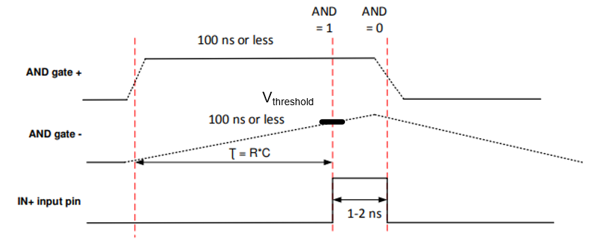 Figure 1-5 Input Buffer Timing Diagram
An alternate way to create a 1ns pulse is by using two input signals for the driver. For this to work, one of the signals will have to be delayed, in the case of Figure 1-6 it is the IN- signal. For reference, the output will follow the IN+ signal when IN- is low. The timing diagram in Figure 1-6 shows that IN+ is the leading signal so it will go high first, which will cause the output to go high as well. After a short delay, the IN- signal will go high and since both driver inputs are high the output will go low. The delay between the two input signals going high, as shown by the red dotted lines in Figure 1-6, will be the time the output is high, therefore if the delay between the two signals going high is 1ns then the output will be high for 1ns. This could then be done repeatedly to generate multiple nanosecond pulses.
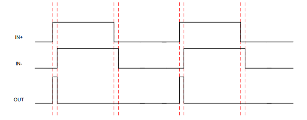 Figure 1-6 Nano Second Pulse Timing Diagram with Delayed Signal
DC/DC Converters Application
Switching regulators are the most efficient way to convert one DC voltage to another DC voltage. DC/DC converter are used for many things such as for step-down (buck) regulators, step-up (boost) regulators, buck-boost regulators, and inverting regulators. Switching-mode power supply designers are always pursuing higher power density, which requires higher frequency and efficiency.
GaN in DC/DC Converter
Compared to Si FETs, GaN high electron mobility transistors (HEMTs) exhibit smaller gate charge, faster switching, and no reverse recovery loss making them more advantageous for switching-mode power supply designers.
An example of the use of GaN for a DC/DC converter can be seen in the TI Design: TIDA-01634. This reference design uses GaN power HEMTs and a latest generation driver, the LMG1210 GaN half-bridge driver, to realize a multi-MHz synchronous buck converter with high efficiency. This buck converter can realize 3 ns of minimum on-time and up to a 50 MHz operation frequency. This design also provides driver UVLO and overtemperature protection.
Applications of TIDA-01634
With high-efficiency switching and flexible dead-time adjustment, this design can significantly improve power density while achieving good efficiency as well as wide control bandwidth.
This design can be applied to many space-constrained and fast response required applications such as high-speed synchronous buck converters, 5G telecom power, 48-to-POL server power, industrial power supplies, Class D audio amplifiers, and envelope tracking.
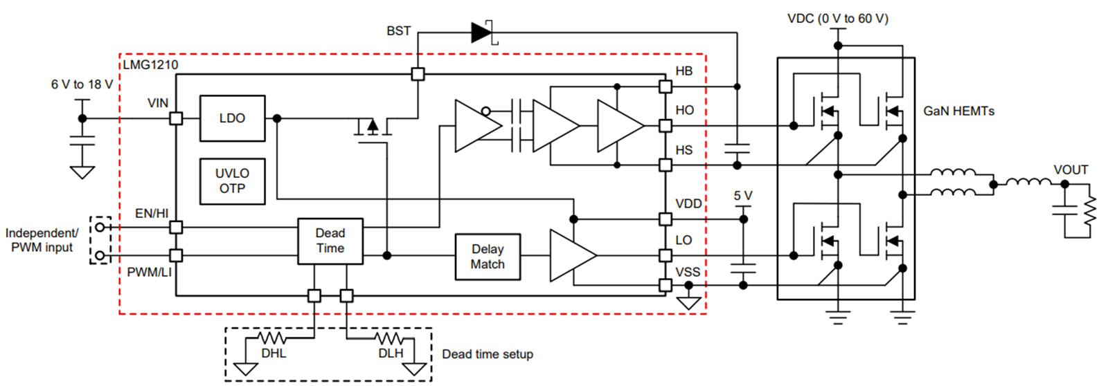 Figure 1-7 Block Diagram of the Synchronous Buck Converter