SLUAAL9 August 2022 LM5113 , LM5113-Q1 , LMG1020 , LMG1025-Q1 , LMG1205 , LMG1210 , UCC27611
Power Loss in Switching Power Supplies
In power switching supplies, one of the primary contributors for power losses are power transistors. Transistor losses stem from two main categories: conduction losses and switching losses.
Conduction losses refer to losses caused by current flow when the power transistor is turned on. Switching losses refer to losses that occur when the transistor is in the process of turning on and off.
Conduction Losses
Similar to Silicon transistors, when turned on, GaN transistors resemble a resistance that is between drain and source. This resistance is often referred to as Rds(on) or Ron. Conduction losses are proportional to this resistance.
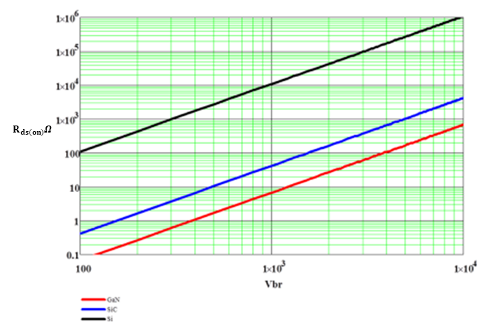
When it comes to the relationship between breakdown voltage and Rds(on), GaN provides a huge advantage over other materials. For a given breakdown voltage, the Rds(on) value of GaN devices is the lowest compared to that of Silicon and Silicon Carbide devices (shown in Figure 1-1). By having lower Rds(on) values than other materials, our conduction losses are also lower.
 Figure 1-1 Breakdown Voltage vs. Rds(on) Graph for Silicon, Silicon Carbide, and Gallium Nitride
Switching Losses
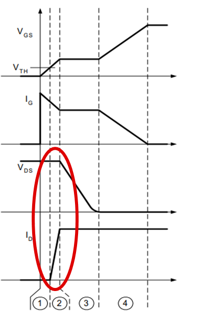
One source of switching losses comes from the time interval during the turn on process in which current in a transistor begins to flow before the drain-to-source voltage begins to drop as shown in Figure 1-2.
 Figure 1-2 Turn-On Process Waveforms
During this time interval the power losses, calculated using Equation 1, are very large.
- IL - the load current
- T - the switching period
- Vds,off - the drain voltage
Increasing the switching speed shortens this time interval, which reduces the losses from this transition.
Given that GaN transistors are able to switch at much faster speeds compared to Silicon transistors, they significantly reduce the losses from the turn on process.
Another way that GaN reduces switching losses is from the absence of a body diode in GaN FETs. To understand how the absence of a body diode in GaN FETs reduces losses, we go through an example of a buck converter using Si MOSFETS.
In a half-bridge configuration, to avoid a short circuit condition called shoot through – which is when both high-side and low-side FETs turn on simultaneously – after one FET turns off, the controller generates a short dead-time before another FET switches on, so both FETs will be off.
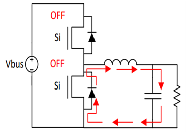
During this dead time, current continues to flow but because both FETs are off, current is forced through the body diode.
 Figure 1-3 Current Path During Dead Time
However, the body diode is much less efficient than the Rds(on) resistance, but Silicon FETs cannot conduct during this time.
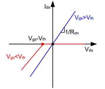
This is where using GaN is beneficial. GaN devices can conduct in the third quadrant with diode like behavior. So, the current that goes through the body diode of a Si MOSFET actually goes through the Rds(on) resistance in a GaN transistor which significantly reduces the losses incurred during dead-time.
 Figure 1-4 Simplified Behavior of GaN in the First and Third Quadrants
In addition, when the body diode of the Si MOSFET turns off after conducting during dead time, current actually flows in the reverse direction for a short period of time which causes additional losses. But since GaN transistors don’t have a body diode, we get almost zero reverse recovery loss.
Form Factor Reduction
It is important to note that operating at higher frequencies leads to smaller passive components since their values are inversely proportional to each other.
While the switching losses during a single switching transition can be large, at lower frequencies (time between each switch is large), the average value of the losses over time can be kept at a safe level.
We just discussed how the switching losses of GaN devices are lower compared to other materials. In this case we can reduce the time between switches. This means we can operate at higher frequencies while keeping the average value of switching losses at a safe level.
Increasing the switching frequency reduces the size of passive components in our devices such as transformers, inductors, and output capacitors which leads to smaller device sizes.
In addition, GaN devices also have better thermal conductivity and can withstand higher temperatures than Silicon. Better thermal conductivity and tolerance reduces the need for thermal management components like large heatsinks, frames, or fans. With these benefits, the overall size of GaN devices is reduced.