ZHCSJN4C February   2018  – February 2020 TPS2HB16-Q1

PRODUCTION DATA.  

  1. 特性
  2. 应用
  3. 说明
    1.     简化原理图
  4. 修订历史记录
  5. Device Comparison Table
  6. Pin Configuration and Functions
    1.     Pin Functions
    2. 6.1 Recommended Connections for Unused Pins
  7. Specifications
    1. Table 3. Absolute Maximum Ratings
    2. Table 4. ESD Ratings
    3. Table 5. Recommended Operating Conditions
    4. Table 6. Thermal Information
    5. Table 7. Electrical Characteristics
    6. Table 8. SNS Timing Characteristics
    7. Table 9. Switching Characteristics
    8. 7.1      Typical Characteristics
  8. Parameter Measurement Information
  9. Detailed Description
    1. 9.1 Overview
    2. 9.2 Functional Block Diagram
    3. 9.3 Feature Description
      1. 9.3.1 Protection Mechanisms
        1. 9.3.1.1 Thermal Shutdown
        2. 9.3.1.2 Current Limit
          1. 9.3.1.2.1 Current Limit Foldback
          2. 9.3.1.2.2 Programmable Current Limit
          3. 9.3.1.2.3 Undervoltage Lockout (UVLO)
          4. 9.3.1.2.4 VBB During Short-to-Ground
        3. 9.3.1.3 Voltage Transients
          1. 9.3.1.3.1 Load Dump
        4. 9.3.1.4 Driving Inductive Loads
        5. 9.3.1.5 Reverse Battery
        6. 9.3.1.6 Fault Event – Timing Diagrams (Version A/B)
      2. 9.3.2 Fault Event – Timing Diagrams - Version F
      3. 9.3.3 Diagnostic Mechanisms
        1. 9.3.3.1 VOUTx Short-to-Battery and Open-Load
          1. 9.3.3.1.1 Detection With Switch Enabled
          2. 9.3.3.1.2 Detection With Switch Disabled
        2. 9.3.3.2 SNS Output
          1. 9.3.3.2.1 RSNS Value
            1. 9.3.3.2.1.1 High Accuracy Load Current Sense
            2. 9.3.3.2.1.2 SNS Output Filter
        3. 9.3.3.3 Fault Indication and SNS Mux
        4. 9.3.3.4 Resistor Sharing
        5. 9.3.3.5 High-Frequency, Low Duty-Cycle Current Sensing
    4. 9.4 Device Functional Modes
      1. 9.4.1 Off
      2. 9.4.2 Standby
      3. 9.4.3 Diagnostic
      4. 9.4.4 Standby Delay
      5. 9.4.5 Active
      6. 9.4.6 Fault
  10. 10Application and Implementation
    1. 10.1 Application Information
      1. 10.1.1 Ground Protection Network
      2. 10.1.2 Interface With Microcontroller
      3. 10.1.3 I/O Protection
      4. 10.1.4 Inverse Current
      5. 10.1.5 Loss of GND
      6. 10.1.6 Automotive Standards
        1. 10.1.6.1 ISO7637-2
        2. 10.1.6.2 AEC – Q100-012 Short Circuit Reliability
      7. 10.1.7 Thermal Information
    2. 10.2 Typical Application
      1. 10.2.1 Design Requirements
      2. 10.2.2 Detailed Design Procedure
      3. 10.2.3 Application Curves
      4. 10.2.4 Design Requirements
      5. 10.2.5 Detailed Design Procedure
      6. 10.2.6 Application Curves
    3. 10.3 Typical Application
      1. 10.3.1 Design Requirements
      2. 10.3.2 Detailed Design Procedure
        1. 10.3.2.1 Thermal Considerations
        2. 10.3.2.2 RILIM Calculation
        3. 10.3.2.3 Diagnostics
          1. 10.3.2.3.1 Selecting the RSNS Value
      3. 10.3.3 Application Curves
  11. 11Power Supply Recommendations
  12. 12Layout
    1. 12.1 Layout Guidelines
    2. 12.2 Layout Example
  13. 13器件和文档支持
    1. 13.1 文档支持
      1. 13.1.1 相关文档
    2. 13.2 接收文档更新通知
    3. 13.3 支持资源
    4. 13.4 商标
    5. 13.5 静电放电警告
    6. 13.6 Glossary
  14. 14机械、封装和可订购信息

Application Curves

When the device receives a rising edge on the ENx pulse the output will turn on as shown in Figure 53. After the turn-on delay time, the device VOUT goes to the VBB supply and begins outputting the steady state resistive current.
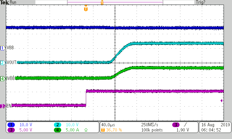
TPS2HB16-Q1 ss1.pngFigure 53. Turn On Waveform

When the device turns off on a falling edge of ENx, the channel IOUT will go to zero and the VOUT will drop to zero as well as shown in Figure 54.
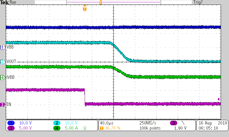
TPS2HB16-Q1 ss2.pngFigure 54. Turn-Off Waveform

While enabled, it is important to measure the output current through both channels. Figure 55 shows this behavior when toggling the SELx pins. The image shows that when SEL2 toggles high to low, the SNS pin toggles between representing IOUT1 and IOUT2. When SEL2 is low SNS represents IOUT1 and when SEL2 is high SNS represents IOUT2. This image shows that channel 2 is currently outputting twice the output current as channel 1.
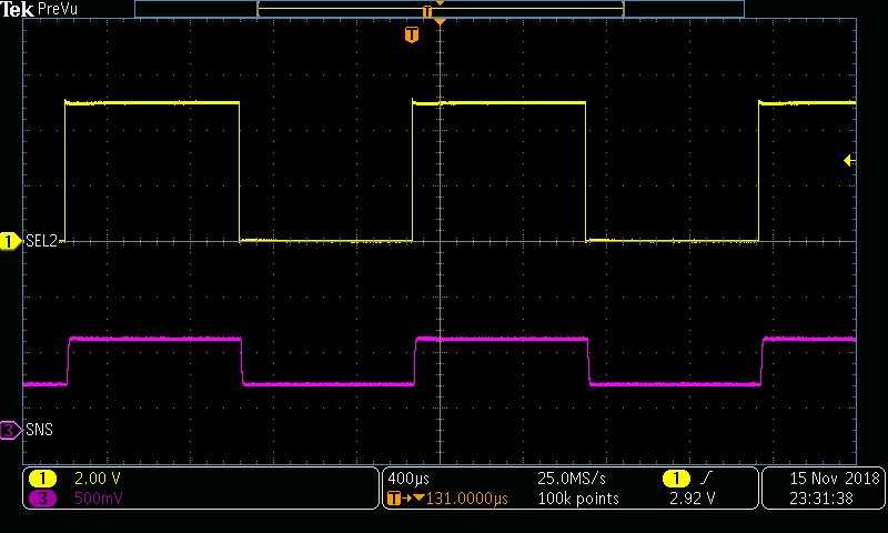
TPS2HB16-Q1 SNS Change Channel.pngFigure 55. Toggling Between CH1 and CH2 Current Measurement

Figure 56 shows the SNS current behavior when there is a load step. The image shows the output current temporarily increase from 1 A to 5 A and then return to 1 A. In this situation, the output current is accurately modeled throughout the pulse by the voltage on the SNS pin allowing for accurate diagnostics.
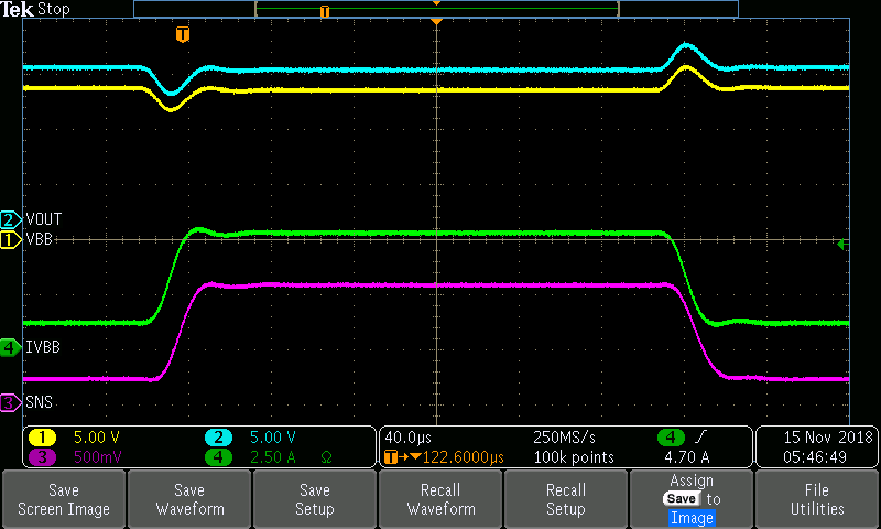
TPS2HB16-Q1 Load Step Settling.pngFigure 56. SNS Settling Time

If the output of the TPS2HB16-Q1 is short-circuited, the device will protect the system from failure. shows the device turning off the output at a set current limit when the output is short circuited. (Note: shows a case with a higher RILIM than calculated in this example, so the current limit is higher than ).
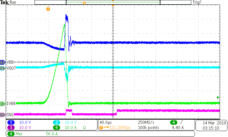
TPS2HB16-Q1 TPS2HB16_B_U2_CH1__VBB=13p5__TEMP=25.pngFigure 57. TPS2HB16B-Q1 Short Circuit Waveform