ZHCSJN4C February   2018  – February 2020 TPS2HB16-Q1

PRODUCTION DATA.  

  1. 特性
  2. 应用
  3. 说明
    1.     简化原理图
  4. 修订历史记录
  5. Device Comparison Table
  6. Pin Configuration and Functions
    1.     Pin Functions
    2. 6.1 Recommended Connections for Unused Pins
  7. Specifications
    1. Table 3. Absolute Maximum Ratings
    2. Table 4. ESD Ratings
    3. Table 5. Recommended Operating Conditions
    4. Table 6. Thermal Information
    5. Table 7. Electrical Characteristics
    6. Table 8. SNS Timing Characteristics
    7. Table 9. Switching Characteristics
    8. 7.1      Typical Characteristics
  8. Parameter Measurement Information
  9. Detailed Description
    1. 9.1 Overview
    2. 9.2 Functional Block Diagram
    3. 9.3 Feature Description
      1. 9.3.1 Protection Mechanisms
        1. 9.3.1.1 Thermal Shutdown
        2. 9.3.1.2 Current Limit
          1. 9.3.1.2.1 Current Limit Foldback
          2. 9.3.1.2.2 Programmable Current Limit
          3. 9.3.1.2.3 Undervoltage Lockout (UVLO)
          4. 9.3.1.2.4 VBB During Short-to-Ground
        3. 9.3.1.3 Voltage Transients
          1. 9.3.1.3.1 Load Dump
        4. 9.3.1.4 Driving Inductive Loads
        5. 9.3.1.5 Reverse Battery
        6. 9.3.1.6 Fault Event – Timing Diagrams (Version A/B)
      2. 9.3.2 Fault Event – Timing Diagrams - Version F
      3. 9.3.3 Diagnostic Mechanisms
        1. 9.3.3.1 VOUTx Short-to-Battery and Open-Load
          1. 9.3.3.1.1 Detection With Switch Enabled
          2. 9.3.3.1.2 Detection With Switch Disabled
        2. 9.3.3.2 SNS Output
          1. 9.3.3.2.1 RSNS Value
            1. 9.3.3.2.1.1 High Accuracy Load Current Sense
            2. 9.3.3.2.1.2 SNS Output Filter
        3. 9.3.3.3 Fault Indication and SNS Mux
        4. 9.3.3.4 Resistor Sharing
        5. 9.3.3.5 High-Frequency, Low Duty-Cycle Current Sensing
    4. 9.4 Device Functional Modes
      1. 9.4.1 Off
      2. 9.4.2 Standby
      3. 9.4.3 Diagnostic
      4. 9.4.4 Standby Delay
      5. 9.4.5 Active
      6. 9.4.6 Fault
  10. 10Application and Implementation
    1. 10.1 Application Information
      1. 10.1.1 Ground Protection Network
      2. 10.1.2 Interface With Microcontroller
      3. 10.1.3 I/O Protection
      4. 10.1.4 Inverse Current
      5. 10.1.5 Loss of GND
      6. 10.1.6 Automotive Standards
        1. 10.1.6.1 ISO7637-2
        2. 10.1.6.2 AEC – Q100-012 Short Circuit Reliability
      7. 10.1.7 Thermal Information
    2. 10.2 Typical Application
      1. 10.2.1 Design Requirements
      2. 10.2.2 Detailed Design Procedure
      3. 10.2.3 Application Curves
      4. 10.2.4 Design Requirements
      5. 10.2.5 Detailed Design Procedure
      6. 10.2.6 Application Curves
    3. 10.3 Typical Application
      1. 10.3.1 Design Requirements
      2. 10.3.2 Detailed Design Procedure
        1. 10.3.2.1 Thermal Considerations
        2. 10.3.2.2 RILIM Calculation
        3. 10.3.2.3 Diagnostics
          1. 10.3.2.3.1 Selecting the RSNS Value
      3. 10.3.3 Application Curves
  11. 11Power Supply Recommendations
  12. 12Layout
    1. 12.1 Layout Guidelines
    2. 12.2 Layout Example
  13. 13器件和文档支持
    1. 13.1 文档支持
      1. 13.1.1 相关文档
    2. 13.2 接收文档更新通知
    3. 13.3 支持资源
    4. 13.4 商标
    5. 13.5 静电放电警告
    6. 13.6 Glossary
  14. 14机械、封装和可订购信息

Pin Configuration and Functions

PWP Package (Version A/B)
16-Pin HTSSOP
Top View
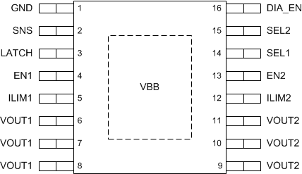
TPS2HB16-Q1 Pinout.gif
PWP Package (Version F)
16-Pin HTSSOP
Top View
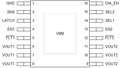
TPS2HB16-Q1 Pinout_F.gif

Pin Functions

PIN I/O DESCRIPTION
NO. Version A/B Version F
GND 1 1 - Device ground
SNS 2 2 O Sense output
LATCH 3 3 I Sets fault handling behavior (latched or auto-retry)
EN1 4 4 I Channel 1 control input, active high
ILIM1 5 - O Connect pull-up resistor to VBB to set current-limit threshold on CH1
FLT1 - 5 O Open drain fault indication
VOUT1 6-8 6-8 O Channel 1 output
VOUT2 9-11 9-11 O Channel 2 output
ILIM2 12 - O Connect pull-up resistor to VBB to set current-limit threshold on CH2
FLT2 - 12 O Open drain fault indication
EN2 13 13 I Channel 2 control input, active high
SEL1 14 14 I Diagnostics select 1. No functionality on version F; tie to device ground through 10 kΩ resistor
SEL2 15 15 I Diagnostics select 2
DIA_EN 16 16 I Diagnostic enable, active high
VBB Exposed Pad Exposed Pad I Power supply input