ZHCSJN4C February   2018  – February 2020 TPS2HB16-Q1

PRODUCTION DATA.  

  1. 特性
  2. 应用
  3. 说明
    1.     简化原理图
  4. 修订历史记录
  5. Device Comparison Table
  6. Pin Configuration and Functions
    1.     Pin Functions
    2. 6.1 Recommended Connections for Unused Pins
  7. Specifications
    1. Table 3. Absolute Maximum Ratings
    2. Table 4. ESD Ratings
    3. Table 5. Recommended Operating Conditions
    4. Table 6. Thermal Information
    5. Table 7. Electrical Characteristics
    6. Table 8. SNS Timing Characteristics
    7. Table 9. Switching Characteristics
    8. 7.1      Typical Characteristics
  8. Parameter Measurement Information
  9. Detailed Description
    1. 9.1 Overview
    2. 9.2 Functional Block Diagram
    3. 9.3 Feature Description
      1. 9.3.1 Protection Mechanisms
        1. 9.3.1.1 Thermal Shutdown
        2. 9.3.1.2 Current Limit
          1. 9.3.1.2.1 Current Limit Foldback
          2. 9.3.1.2.2 Programmable Current Limit
          3. 9.3.1.2.3 Undervoltage Lockout (UVLO)
          4. 9.3.1.2.4 VBB During Short-to-Ground
        3. 9.3.1.3 Voltage Transients
          1. 9.3.1.3.1 Load Dump
        4. 9.3.1.4 Driving Inductive Loads
        5. 9.3.1.5 Reverse Battery
        6. 9.3.1.6 Fault Event – Timing Diagrams (Version A/B)
      2. 9.3.2 Fault Event – Timing Diagrams - Version F
      3. 9.3.3 Diagnostic Mechanisms
        1. 9.3.3.1 VOUTx Short-to-Battery and Open-Load
          1. 9.3.3.1.1 Detection With Switch Enabled
          2. 9.3.3.1.2 Detection With Switch Disabled
        2. 9.3.3.2 SNS Output
          1. 9.3.3.2.1 RSNS Value
            1. 9.3.3.2.1.1 High Accuracy Load Current Sense
            2. 9.3.3.2.1.2 SNS Output Filter
        3. 9.3.3.3 Fault Indication and SNS Mux
        4. 9.3.3.4 Resistor Sharing
        5. 9.3.3.5 High-Frequency, Low Duty-Cycle Current Sensing
    4. 9.4 Device Functional Modes
      1. 9.4.1 Off
      2. 9.4.2 Standby
      3. 9.4.3 Diagnostic
      4. 9.4.4 Standby Delay
      5. 9.4.5 Active
      6. 9.4.6 Fault
  10. 10Application and Implementation
    1. 10.1 Application Information
      1. 10.1.1 Ground Protection Network
      2. 10.1.2 Interface With Microcontroller
      3. 10.1.3 I/O Protection
      4. 10.1.4 Inverse Current
      5. 10.1.5 Loss of GND
      6. 10.1.6 Automotive Standards
        1. 10.1.6.1 ISO7637-2
        2. 10.1.6.2 AEC – Q100-012 Short Circuit Reliability
      7. 10.1.7 Thermal Information
    2. 10.2 Typical Application
      1. 10.2.1 Design Requirements
      2. 10.2.2 Detailed Design Procedure
      3. 10.2.3 Application Curves
      4. 10.2.4 Design Requirements
      5. 10.2.5 Detailed Design Procedure
      6. 10.2.6 Application Curves
    3. 10.3 Typical Application
      1. 10.3.1 Design Requirements
      2. 10.3.2 Detailed Design Procedure
        1. 10.3.2.1 Thermal Considerations
        2. 10.3.2.2 RILIM Calculation
        3. 10.3.2.3 Diagnostics
          1. 10.3.2.3.1 Selecting the RSNS Value
      3. 10.3.3 Application Curves
  11. 11Power Supply Recommendations
  12. 12Layout
    1. 12.1 Layout Guidelines
    2. 12.2 Layout Example
  13. 13器件和文档支持
    1. 13.1 文档支持
      1. 13.1.1 相关文档
    2. 13.2 接收文档更新通知
    3. 13.3 支持资源
    4. 13.4 商标
    5. 13.5 静电放电警告
    6. 13.6 Glossary
  14. 14机械、封装和可订购信息

Thermal Information

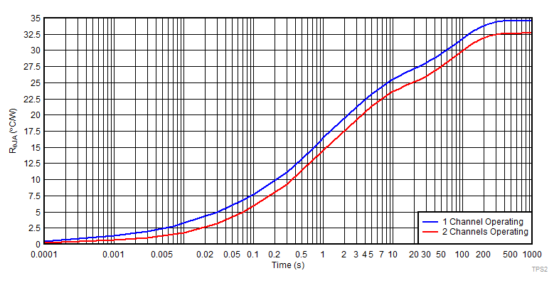
When outputting current, the TPS2HB16-Q1 will heat up due to the power dissipation. The transient thermal impedance curve can be used to determine the device temperature during a pulse of a given length. This RθJA value corresponds to a JEDEC standard 2s2p thermal test PCB with thermal vias. The RθJA will vary depending on whether the power dissipation is concentrated in a single channel or is distributed evenly between each channel.
TPS2HB16-Q1 TPS2HB16RC.gifFigure 47. TPS2HB16-Q1 Transient Thermal Impedance