ZHCSIK3 July   2018 TPS650861

PRODUCTION DATA.  

  1. 1器件概述
    1. 1.1 特性
    2. 1.2 应用
    3. 1.3 说明
    4. 1.4 PMIC 功能框图
  2. 2修订历史记录
  3. 3Pin Configuration and Functions
    1. 3.1 Pin Functions
      1.      Pin Functions
  4. 4Specifications
    1. 4.1  Absolute Maximum Ratings
    2. 4.2  ESD Ratings
    3. 4.3  Recommended Operating Conditions
    4. 4.4  Thermal Information
    5. 4.5  Electrical Characteristics: Total Current Consumption
    6. 4.6  Electrical Characteristics: Reference and Monitoring System
    7. 4.7  Electrical Characteristics: Buck Controllers
    8. 4.8  Electrical Characteristics: Synchronous Buck Converters
    9. 4.9  Electrical Characteristics: LDOs
    10. 4.10 Electrical Characteristics: Load Switches
    11. 4.11 Digital Signals: I2C Interface
    12. 4.12 Digital Input Signals (CTLx)
    13. 4.13 Digital Output Signals (IRQB, GPOx)
    14. 4.14 Timing Requirements
    15. 4.15 Switching Characteristics
    16. 4.16 Typical Characteristics
  5. 5Detailed Description
    1. 5.1  Overview
    2. 5.2  Functional Block Diagram
    3. 5.3  Programming the TPS650861
    4. 5.4  SMPS Voltage Regulators
      1. 5.4.1 Controller Overview
      2. 5.4.2 Converter Overview
      3. 5.4.3 DVS
      4. 5.4.4 Decay
      5. 5.4.5 Current Limit
    5. 5.5  LDOs and Load Switches
      1. 5.5.1 VTT LDO
      2. 5.5.2 LDOA1–LDOA3
      3. 5.5.3 Load Switches
    6. 5.6  Power Goods (PGOOD or PG) and GPOs
    7. 5.7  One-Time Programmable Memory
    8. 5.8  Power Sequencing and VR Control
      1. 5.8.1 CTLx Sequencing
      2. 5.8.2 PG Sequencing
      3. 5.8.3 Enable Delay
      4. 5.8.4 Power-Up Sequence
      5. 5.8.5 Power-Down Sequence
      6. 5.8.6 Sleep State Entry and Exit
      7. 5.8.7 Emergency Shutdown
    9. 5.9  Device Functional Modes
      1. 5.9.1 Off Mode
      2. 5.9.2 Standby Mode
      3. 5.9.3 Active Mode
    10. 5.10 I2C Interface
      1. 5.10.1 F/S-Mode Protocol
    11. 5.11 I2C Address: 0x5E Register Maps
      1. 5.11.1  Register Map Summary
      2. 5.11.2  DEVICEID1: 1st PMIC Device and Revision ID Register (offset = 00h) [reset = X]
        1. Table 5-8 DEVICEID1 Register Descriptions
      3. 5.11.3  DEVICEID2: 2nd PMIC Device and Revision ID Register (offset = 01h) [reset = X]
        1. Table 5-9 DEVICEID2 Register Descriptions
      4. 5.11.4  IRQ: PMIC Interrupt Register (offset = 02h) [reset = 0000 0000]
        1. Table 5-10 IRQ Register Descriptions
      5. 5.11.5  IRQ_MASK: PMIC Interrupt Mask Register (offset = 03h) [reset = 1111 1111]
        1. Table 5-11 IRQ_MASK Register Descriptions
      6. 5.11.6  PMICSTAT: PMIC Status Register (offset = 04h) [reset = 0000 0000]
        1. Table 5-12 PMICSTAT Register Descriptions
      7. 5.11.7  SHUTDNSRC: PMIC Shut-Down Event Register (offset = 05h) [reset = 0000 0000]
        1. Table 5-13 SHUTDNSRC Register Descriptions
      8. 5.11.8  BUCK1CTRL: BUCK1 Control Register (offset = 20h) [reset = X]
        1. Table 5-14 BUCK1CTRL Register Descriptions
      9. 5.11.9  BUCK2CTRL: BUCK2 Control Register (offset = 21h) [reset = X]
        1. Table 5-15 BUCK2CTRL Register Descriptions
      10. 5.11.10 BUCK3DECAY: BUCK3 Decay Control Register (offset = 22h) [reset = X]
        1. Table 5-16 BUCK3DECAY Register Descriptions
      11. 5.11.11 BUCK3VID: BUCK3 VID Register (offset = 23h) [reset = X]
        1. Table 5-17 BUCK3VID Register Descriptions
      12. 5.11.12 BUCK3SLPCTRL: BUCK3 Sleep Control VID Register (offset = 24h) [reset = X]
        1. Table 5-18 BUCK3SLPCTRL Register Descriptions
      13. 5.11.13 BUCK4CTRL: BUCK4 Control Register (offset = 25h) [reset = X]
        1. Table 5-19 BUCK4CTRL Register Descriptions
      14. 5.11.14 BUCK5CTRL: BUCK5 Control Register (offset = 26h) [reset = X]
        1. Table 5-20 BUCK5CTRL Register Descriptions
      15. 5.11.15 BUCK6CTRL: BUCK6 Control Register (offset = 27h) [reset = X]
        1. Table 5-21 BUCK6CTRL Register Descriptions
      16. 5.11.16 LDOA2CTRL: LDOA2 Control Register (offset = 28h) [reset = X]
        1. Table 5-22 LDOA2CTRL Register Descriptions
      17. 5.11.17 LDOA3CTRL: LDOA3 Control Register (offset = 29h) [reset = X]
        1. Table 5-23 LDOA3CTRL Register Descriptions
      18. 5.11.18 DISCHCTRL1: 1st Discharge Control Register (offset = 40h) [reset = X]
        1. Table 5-24 DISCHCTRL1 Register Descriptions
      19. 5.11.19 DISCHCTRL2: 2nd Discharge Control Register (offset = 41h) [reset = X]
        1. Table 5-25 DISCHCTRL2 Register Descriptions
      20. 5.11.20 DISCHCTRL3: 3rd Discharge Control Register (offset = 42h) [reset = X]
        1. Table 5-26 DISCHCTRL3 Register Descriptions
      21. 5.11.21 PG_DELAY1: 1st Power Good Delay Register (offset = 43h) [reset = X]
        1. Table 5-27 PG_DELAY1 Register Descriptions
      22. 5.11.22 FORCESHUTDN: Force Emergency Shutdown Control Register (offset = 91h) [reset = 0000 0000]
        1. Table 5-28 FORCESHUTDN Register Descriptions
      23. 5.11.23 BUCK1SLPCTRL: BUCK1 Sleep Control Register (offset = 92h) [reset = X]
        1. Table 5-29 BUCK1SLPCTRL Register Descriptions
      24. 5.11.24 BUCK2SLPCTRL: BUCK2 Sleep Control Register (offset = 93h) [reset = X]
        1. Table 5-30 BUCK2SLPCTRL Register Descriptions
      25. 5.11.25 BUCK4VID: BUCK4 VID Register (offset = 94h) [reset = X]
        1. Table 5-31 BUCK4VID Register Descriptions
      26. 5.11.26 BUCK4SLPVID: BUCK4 Sleep VID Register (offset = 95h) [reset = X]
        1. Table 5-32 BUCK4SLPVID Register Descriptions
      27. 5.11.27 BUCK5VID: BUCK5 VID Register (offset = 96h) [reset = X]
        1. Table 5-33 BUCK5VID Register Descriptions
      28. 5.11.28 BUCK5SLPVID: BUCK5 Sleep VID Register (offset = 97h) [reset = X]
        1. Table 5-34 BUCK5SLPVID Register Descriptions
      29. 5.11.29 BUCK6VID: BUCK6 VID Register (offset = 98h) [reset = X]
        1. Table 5-35 BUCK6VID Register Descriptions
      30. 5.11.30 BUCK6SLPVID: BUCK6 Sleep VID Register (offset = 99h) [reset = X]
        1. Table 5-36 BUCK6SLPVID Register Descriptions
      31. 5.11.31 LDOA2VID: LDOA2 VID Register (offset = 9Ah) [reset = X]
        1. Table 5-37 LDOA2VID Register Descriptions
      32. 5.11.32 LDOA3VID: LDOA3 VID Register (offset = 9Bh) [reset = X]
        1. Table 5-38 LDOA3VID Register Descriptions
      33. 5.11.33 BUCK123CTRL: BUCK1-3 Control Register (offset = 9Ch) [reset = X]
        1. Table 5-39 BUCK123CTRL Register Descriptions
      34. 5.11.34 PG_DELAY2: 2nd Power Good Delay Register (offset = 9Dh) [reset = X]
        1. Table 5-40 PG_DELAY2 Register Descriptions
      35. 5.11.35 SWVTT_DIS: SWVTT Disable Register (offset = 9Fh) [reset = X]
        1. Table 5-41 SWVTT_DIS Register Descriptions
      36. 5.11.36 I2C_RAIL_EN1: 1st VR Pin Enable Override Register (offset = A0h) [reset = X]
        1. Table 5-42 I2C_RAIL_EN1 Register Descriptions
      37. 5.11.37 I2C_RAIL_EN2/GPOCTRL: 2nd VR Pin Enable Override and GPO Control Register (offset = A1h) [reset = X]
        1. Table 5-43 I2C_RAIL_EN2/GPOCTRL Register Descriptions
      38. 5.11.38 PWR_FAULT_MASK1: 1st VR Power Fault Mask Register (offset = A2h) [reset = X]
        1. Table 5-44 PWR_FAULT_MASK1 Register Descriptions
      39. 5.11.39 PWR_FAULT_MASK2: 2nd VR Power Fault Mask Register (offset = A3h) [reset = X]
        1. Table 5-45 PWR_FAULT_MASK2 Register Descriptions
      40. 5.11.40 GPO1PG_CTRL1: 1st GPO1 PG Control Register (offset = A4h) [reset = X]
        1. Table 5-46 GPO1PG_CTRL1 Register Descriptions
      41. 5.11.41 GPO1PG_CTRL2: 2nd GPO1 PG Control Register (offset = A5h) [reset = X]
        1. Table 5-47 GPO1PG_CTRL2 Register Descriptions
      42. 5.11.42 GPO4PG_CTRL1: 1st GPO4 PG Control Register (offset = A6h) [reset = X]
        1. Table 5-48 GPO4PG_CTRL1 Register Descriptions
      43. 5.11.43 GPO4PG_CTRL2: 2nd GPO4 PG Control Register (offset = A7h) [reset = X]
        1. Table 5-49 GPO4PG_CTRL2 Register Descriptionsr
      44. 5.11.44 GPO2PG_CTRL1: 1st GPO2 PG Control Register (offset = A8h) [reset = X]
        1. Table 5-50 GPO2PG_CTRL1 Register Descriptions
      45. 5.11.45 GPO2PG_CTRL2: 2nd GPO2 PG Control Register (offset = A9h) [reset = X]
        1. Table 5-51 GPO2PG_CTRL2 Register Descriptions
      46. 5.11.46 GPO3PG_CTRL1: 1st GPO3 PG Control Register (offset = AAh) [reset = X]
        1. Table 5-52 GPO3PG_CTRL1 Register Descriptions
      47. 5.11.47 GPO3PG_CTRL2: 2nd GPO3 PG Control Register (offset = ABh) [reset = X]
        1. Table 5-53 GPO3PG_CTRL2 Register Descriptions
      48. 5.11.48 MISCSYSPG Register (offset = ACh) [reset = X]
        1. Table 5-54 MISCSYSPG Register Descriptions
        2. 5.11.48.1   VTT_DISCH_CTRL Register (offset = ADh) [reset = X]
          1. Table 5-55 VTT_DISCH_CTRL Register Descriptions
      49. 5.11.49 LDOA1_SWB2_CTRL: LDOA1 and SWB2 Control Register (offset = AEh) [reset = X]
        1. Table 5-56 LDOA1_SWB2_CTRL Register Descriptions
      50. 5.11.50 PG_STATUS1: 1st Power Good Status Register (offset = B0h) [reset = 0000 0000]
        1. Table 5-57 PG_STATUS1 Register Descriptions
      51. 5.11.51 PG_STATUS2: 2nd Power Good Status Register (offset = B1h) [reset = 0000 0000]
        1. Table 5-58 PG_STATUS2 Register Descriptions
      52. 5.11.52 PWR_FAULT_STATUS1: 1st Power Fault Status Register (offset = B2h) [reset = 0000 0000]
        1. Table 5-59 PWR_FAULT_STATUS1 Register Descriptions
      53. 5.11.53 PWR_FAULT_STATUS2: 2nd Power Fault Status Register (offset = B3h) [reset = 0000 0000]
        1. Table 5-60 PWR_FAULT_STATUS2 Register Descriptions
      54. 5.11.54 TEMPCRIT: Temperature Fault Status Register (offset = B4h) [reset = 0000 0000]
        1. Table 5-61 TEMPCRIT Register Descriptions
      55. 5.11.55 TEMPHOT: Temperature Hot Status Register (offset = B5h) [reset = 0000 0000]
        1. Table 5-62 TEMPHOT Register Descriptions
      56. 5.11.56 OC_STATUS: Overcurrent Fault Status Register (offset = B6h) [reset = 0000 0000]
        1. Table 5-63 OC_STATUS Register Descriptions
    12. 5.12 I2C Address: 0x38 Register Maps
      1. 5.12.1  Register Map Summary
      2. 5.12.2  OTP_CTRL1 (offset = 02h) [reset = 0010 0000]
        1. Table 5-65 OTP_CTRL1 Register Descriptions
      3. 5.12.3  OTP_CTRL2 (offset = 03h) [reset = X]
        1. Table 5-66 OTP_CTRL2 Register Descriptions
      4. 5.12.4  BUCK1_CTRL_EN1 (offset = 07h) [reset = X]
        1. Table 5-67 BUCK1_CTRL_EN1 Register Descriptions
      5. 5.12.5  BUCK1_CTRL_EN2 (offset = 08h) [reset = X]
        1. Table 5-68 BUCK1_CTRL_EN2 Register Descriptions
      6. 5.12.6  BUCK1_CTRL_EN3 (offset = 09h) [reset = X]
        1. Table 5-69 BUCK1_CTRL_EN3 Register Descriptions
      7. 5.12.7  BUCK2_CTRL_EN1 (offset = 0Ah) [reset = X]
        1. Table 5-70 BUCK2_CTRL_EN1 Register Descriptions
      8. 5.12.8  BUCK2_CTRL_EN2 (offset = 0Bh) [reset = X]
        1. Table 5-71 BUCK2_CTRL_EN2 Register Descriptions
      9. 5.12.9  BUCK2_CTRL_EN3 (offset = 0Ch) [reset = X]
        1. Table 5-72 BUCK2_CTRL_EN3 Register Descriptions
      10. 5.12.10 BUCK3_CTRL_EN1 (offset = 0Ah) [reset = X]
        1. Table 5-73 BUCK3_CTRL_EN1 Register Descriptions
      11. 5.12.11 BUCK3_CTRL_EN2 (offset = 0Eh) [reset = X]
        1. Table 5-74 BUCK3_CTRL_EN2 Register Descriptions
      12. 5.12.12 BUCK3_CTRL_EN3 (offset = 0Fh) [reset = X]
        1. Table 5-75 BUCK3_CTRL_EN3 Register Descriptions
      13. 5.12.13 BUCK4_CTRL_EN1 (offset = 10h) [reset = X]
        1. Table 5-76 BUCK4_CTRL_EN1 Register Descriptions
      14. 5.12.14 BUCK4_CTRL_EN2 (offset = 11h) [reset = X]
        1. Table 5-77 BUCK4_CTRL_EN2 Register Descriptions
      15. 5.12.15 BUCK4_CTRL_EN3 (offset = 12h) [reset = X]
        1. Table 5-78 BUCK4_CTRL_EN3 Register Descriptions
      16. 5.12.16 BUCK5_CTRL_EN1 (offset = 13h) [reset = X]
        1. Table 5-79 BUCK5_CTRL_EN1 Register Descriptions
      17. 5.12.17 BUCK5_CTRL_EN2 (offset = 14h) [reset = X]
        1. Table 5-80 BUCK5_CTRL_EN2 Register Descriptions
      18. 5.12.18 BUCK5_CTRL_EN3 (offset = 15h) [reset = X]
        1. Table 5-81 BUCK5_CTRL_EN3 Register Descriptions
      19. 5.12.19 BUCK6_CTRL_EN1 (offset = 16h) [reset = X]
        1. Table 5-82 BUCK6_CTRL_EN1 Register Descriptions
      20. 5.12.20 BUCK6_CTRL_EN2 (offset = 17h) [reset = X]
        1. Table 5-83 BUCK6_CTRL_EN2 Register Descriptions
      21. 5.12.21 BUCK6_CTRL_EN3 (offset = 18h) [reset = X]
        1. Table 5-84 BUCK6_CTRL_EN3 Register Descriptions
      22. 5.12.22 SWA1_CTRL_EN1 (offset = 19h) [reset = X]
        1. Table 5-85 SWA1_CTRL_EN1 Register Descriptions
      23. 5.12.23 SWA1_CTRL_EN2 (offset = 1Ah) [reset = X]
        1. Table 5-86 SWA1_CTRL_EN2 Register Descriptions
      24. 5.12.24 SWA1_CTRL_EN3 (offset = 1Bh) [reset = X]
        1. Table 5-87 SWA1_CTRL_EN3 Register Descriptions
      25. 5.12.25 LDOA2_CTRL_EN1 (offset = 1Ch) [reset = X]
        1. Table 5-88 LDOA2_CTRL_EN1 Register Descriptions
      26. 5.12.26 LDOA2_CTRL_EN2 (offset = 1Dh) [reset = X]
        1. Table 5-89 LDOA2_CTRL_EN2 Register Descriptions
      27. 5.12.27 LDOA2_CTRL_EN3 (offset = 1Eh) [reset = X]
        1. Table 5-90 LDOA2_CTRL_EN3 Register Descriptions
      28. 5.12.28 LDOA3_CTRL_EN1 (offset = 1Fh) [reset = X]
        1. Table 5-91 LDOA3_CTRL_EN1 Register Descriptions
      29. 5.12.29 LDOA3_CTRL_EN2 (offset = 20h) [reset = X]
        1. Table 5-92 LDOA3_CTRL_EN2 Register Descriptions
      30. 5.12.30 LDOA3_CTRL_EN3 (offset = 21h) [reset = X]
        1. Table 5-93 LDOA3_CTRL_EN3 Register Descriptions
      31. 5.12.31 SWB1_CTRL_EN1 (offset = 22h) [reset = X]
        1. Table 5-94 SWB1_CTRL_EN1 Register Descriptions
      32. 5.12.32 SWB1_CTRL_EN2 (offset = 23h) [reset = X]
        1. Table 5-95 SWB1_CTRL_EN2 Register Descriptions
      33. 5.12.33 SWB1_CTRL_EN3 (offset = 24h) [reset = X]
        1. Table 5-96 SWB1_CTRL_EN3 Register Descriptions
      34. 5.12.34 SWB2_LDOA1_CTRL_EN1 (offset = 25h) [reset = X]
        1. Table 5-97 SWB2_LDOA1_CTRL_EN1 Register Descriptions
      35. 5.12.35 SWB2_LDOA1_CTRL_EN2 (offset = 26h) [reset = X]
        1. Table 5-98 SWB2_LDOA1_CTRL_EN2 Register Descriptions
      36. 5.12.36 SWB2_LDOA1_CTRL_EN3 (offset = 27h) [reset = X]
        1. Table 5-99 SWB2_LDOA1_CTRL_EN3 Register Descriptions
      37. 5.12.37 SLP_PIN (offset = 29h) [reset = X]
        1. Table 5-100 SLP_PIN Register Descriptions
      38. 5.12.38 OUTPUT_MODE (offset = 2Ah) [reset = X]
        1. Table 5-101 OUTPUT_MODE Register Descriptions
      39. 5.12.39 I2C_SLAVE_ADDR (offset = 5Fh) [reset = X]
        1. Table 5-102 I2C_SLAVE_ADDR Register Descriptions
  6. 6Applications, Implementation, and Layout
    1. 6.1 Application Information
    2. 6.2 Typical Application
      1. 6.2.1 Typical Application Example
        1. 6.2.1.1 Design Requirements
        2. 6.2.1.2 Detailed Design Procedure
          1. 6.2.1.2.1 Controller Design Procedure
            1. 6.2.1.2.1.1 Selecting the Inductor
            2. 6.2.1.2.1.2 Selecting the Output Capacitors
            3. 6.2.1.2.1.3 Selecting the FETs
            4. 6.2.1.2.1.4 Bootstrap Capacitor
            5. 6.2.1.2.1.5 Setting the Current Limit
            6. 6.2.1.2.1.6 Selecting the Input Capacitors
          2. 6.2.1.2.2 Converter Design Procedure
            1. 6.2.1.2.2.1 Selecting the Inductor
            2. 6.2.1.2.2.2 Selecting the Output Capacitors
            3. 6.2.1.2.2.3 Selecting the Input Capacitors
          3. 6.2.1.2.3 LDO Design Procedure
        3. 6.2.1.3 Application Curves
        4. 6.2.1.4 Layout
          1. 6.2.1.4.1 Layout Guidelines
          2. 6.2.1.4.2 Layout Example
      2. 6.2.2 VIN 5-V Application
        1. 6.2.2.1 Design Requirements
        2. 6.2.2.2 Design Procedure
        3. 6.2.2.3 Application Curves
    3. 6.3 Power Supply Coupling and Bulk Capacitors
    4. 6.4 Do's and Don'ts
  7. 7器件和文档支持
    1. 7.1 器件支持
      1. 7.1.1 开发支持
    2. 7.2 文档支持
      1. 7.2.1 相关文档
    3. 7.3 接收文档更新通知
    4. 7.4 社区资源
    5. 7.5 商标
    6. 7.6 静电放电警告
    7. 7.7 术语表
  8. 8机械、封装和可订购信息

Typical Characteristics

Measurements are taken at 25°C.
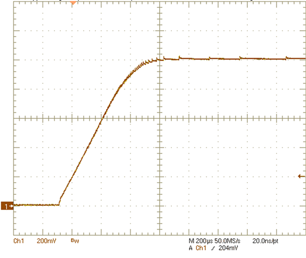
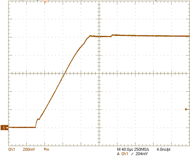
TPS650861 AC_03_swcs129.gif
FET = CSD87588N L = PIMB061H-R22ms
BUCK2_MODE = 0b COUT = 2 × 150 µF + 1 × 22 µF
Figure 4-1 Example BUCK2 Controller Start-Up
TPS650861 D011_SWCS128.gif
FET = CSD87381P L = PIMB061H-R47ms
BUCK1_MODE = 0b
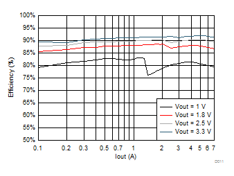
Figure 4-3 Example BUCK1 Efficiency at VIN = 13 V In Auto Mode
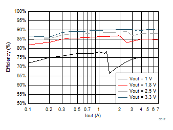
TPS650861 D012_SWCS128.gif
FET = CSD87381P L = PIMB061H-R47ms
BUCK1_MODE = 0b
Figure 4-5 Example BUCK1 Efficiency at VIN = 18 V In Auto Mode
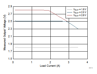
TPS650861 D014_SWCS138.gif
L = PIFE32251B-R47ms
Figure 4-7 Converter Load Current Limitations with VIN = 3.3 V
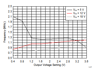
TPS650861 tps65086100-controller-frequency-pwm-curve.gif
FET = CSD87381P L = PIMB061H-R47ms
BUCK1_MODE = 1b
Figure 4-9 Controller Switching Frequency (Forced PWM Mode)
TPS650861 AC_04_swcs129.gif
BUCK3_MODE = 0b L = PIFE32251B-R47ms
COUT = 4 × 22 µF
Figure 4-2 Example BUCK3 Converter Start-Up
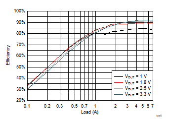
TPS650861 tps65086100-efficiency-13-Vin-curve.gif
FET = CSD87381P L = PIMB061H-R47ms
BUCK1_MODE = 1b
Figure 4-4 Example BUCK1 Efficiency at VIN = 13 V in Forced PWM Mode
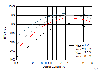
TPS650861 tps65086100-efficiency-buck3-5vin-curve.gif
L = PIFE32251B-R47ms
Figure 4-6 Example BUCK3 Efficiency at VIN = 5 V
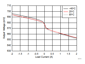
TPS650861 D015_SWCS138.gif
FBVOUT6 = PVINVTT = 1.35 V
Figure 4-8 VTT LDO Regulation
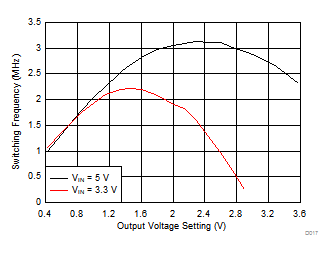
TPS650861 D017_SWCS138.gif
L = PIFE32251B-R47ms
Figure 4-10 Converter Switching Frequency